線上影音
Home > ANSYS SIwave教學> PI Optimize I
The article (part I) is available from 2012 and is rewritten on 2014. It is intended to introduce a traditional PI optimization flow (following Ansoft 2008 presentation), near field、far field simulation using SIwave 2014+HFSS 2014 (data link), and explain the effect of pin group on PI analysis.
2014年更新的部分在於以HFSS data link SIwave near field時,HFSS使用direct solver與PML,incident wave使用incident field,可以得到比較好的結果(step1.8.7)。閱讀本文的同時,建議參考本站另一專文,熟悉做push excitation與plot far field的方法。
-
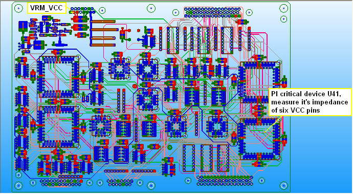
Extract VCC PDN from VRM to Critical Device
1.5 Z-profile
1.7 Time and Frequency Domain
1.8 Near、Far Field by SIwave and HFSS
-
Add Bulk Capacitor (100uF)
-
Add decoupling Capacitor (10nF)
-
Add HF capacitor (2.2nF+3.9nF)
-
問題與討論
12.1 step1.8為何SIwave與HFSS跑出的Far Field不同?
12.2 如何把HFSS跑出的結果,單位從dB換算成dBuV?
12.3 SIwave中,step1.8.5 far field plot的MaxETotal與ETotal有何差別?
12.4 HFSS中,Radiation Boundary的屬性,設[Incident Field]與[Enforced Field]有何差別?
12.5 大部分的板子,其實PI不用設計到如此辛苦,我們取VDD*10%來推算PI design spec.是否過於嚴苛?
12.6 step10.4下電容把VCC impedance降低後,雖然VCC上的Vpp降低,但VCC current會出現非週期性低頻成份?
12.7 Capacitor Library Browser可選擇頻寬、ESR、ESL適合的電容,但為何Z-profile中所示的諧振點(谷點)與SRF頻點不同?
12.8 step9.3加四顆電容就近放在U41 pin,在100MHz新增一個拉低的頻點(谷點),但左側62MHz卻新增一個拉高的頻點(峰點)?
12.9 為何此例中,100MHz以上的PDN impedance特別難壓下來(step 9.1),必須把電容直接下在IC pin上才能看到效果(step 9.2)?
PDN (Power Distribution Network),PDS (Power Distribution System)
![]()
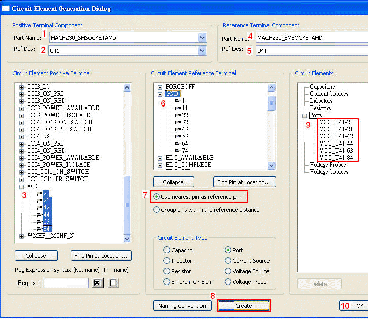
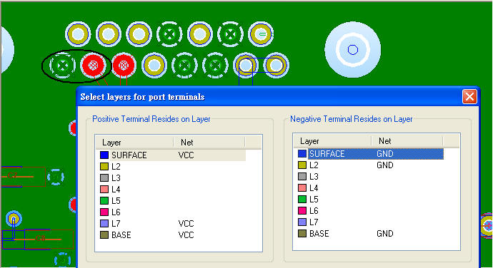
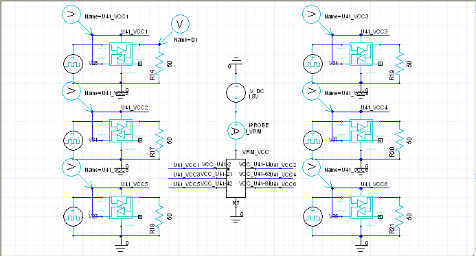
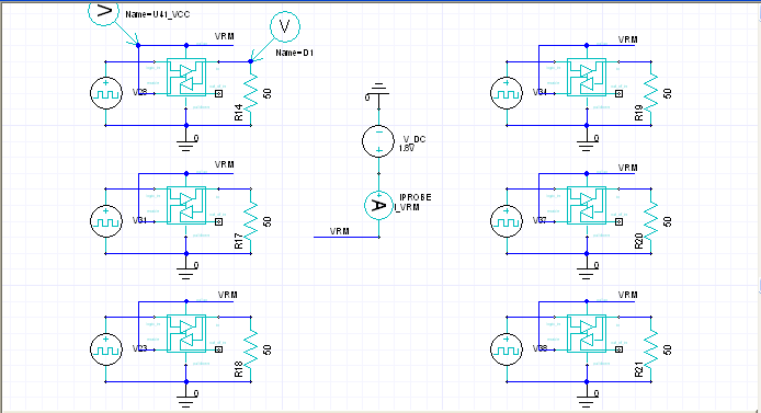
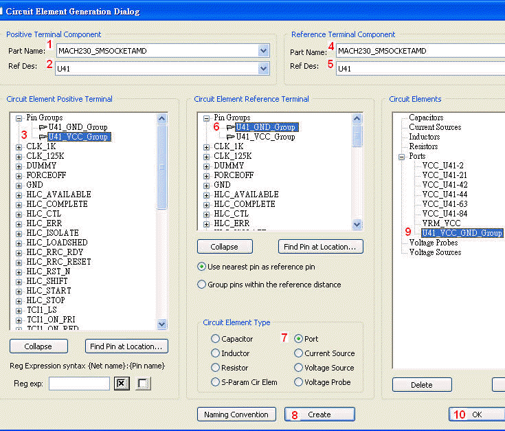
1.1 Add six VCC-GND ports for U41 VCC pins:Circuit Elements \ Generate on Components
1.2 Add one VRM port for VCC:Circuit Elements \ Port
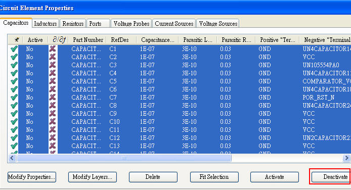
1.3 De-active all the decoupling capacitors at the first
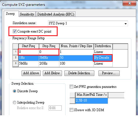
1.4 Compute SYZ-parameters
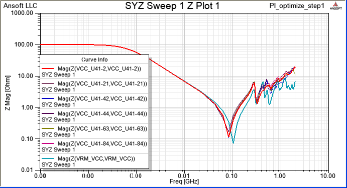
1.5 The original Z-profile as below (bare board impedance)
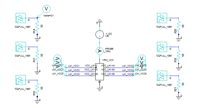
1.6 Export PDN S-parameter from SIwave and use it with DDR2 IBIS in Designer as below
1.6.1 Here is the schematic with old IO symbol
1.6.2 Here is another schematic with new IO symbol (available from Designer 8) 圖面簡潔許多
Use DDR2_1066 full drive IBIS model, and input patterns are 800 Mbps data rate PRBS
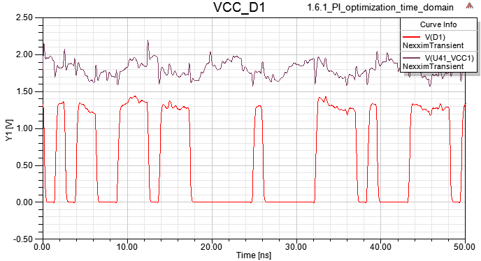
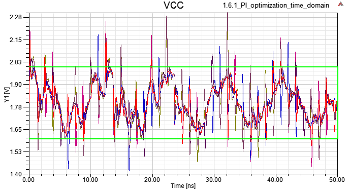
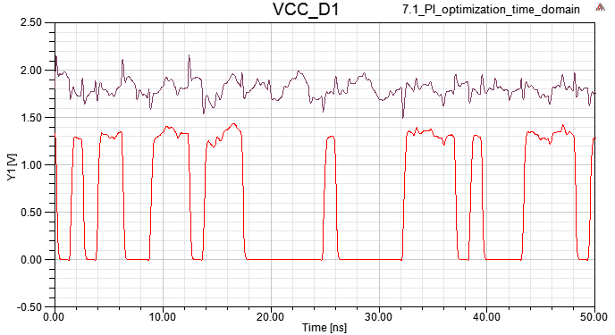
1.7 Driver output and U41 VCC in time domain are showed as below
1.8 Near and Far Field Simulation
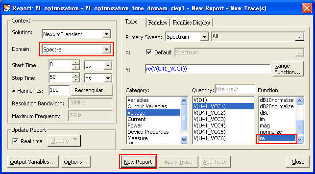
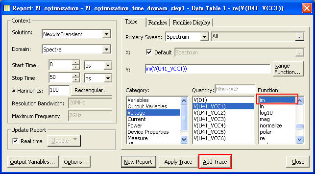
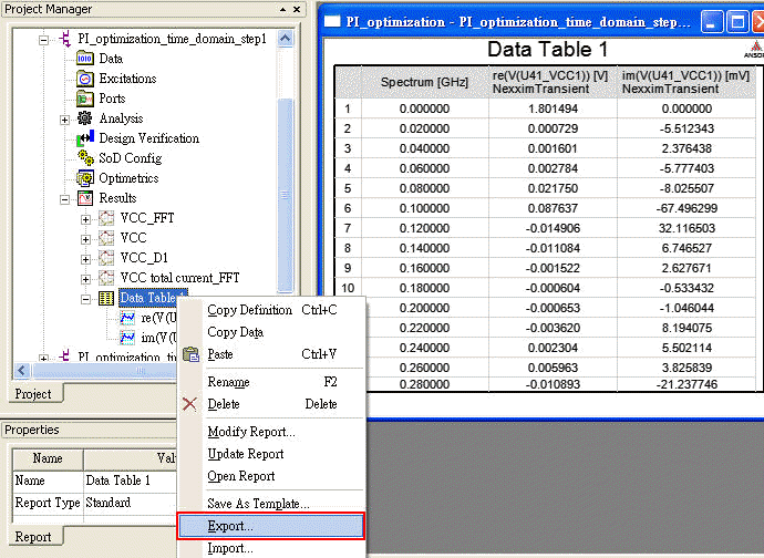
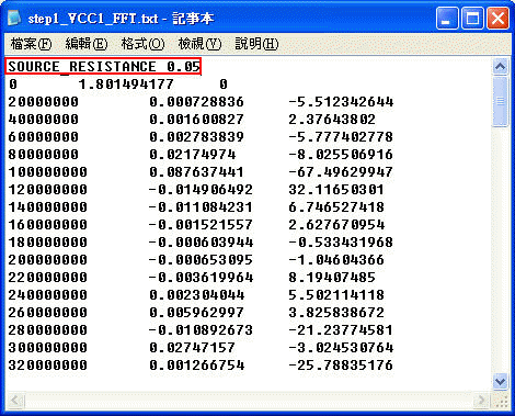
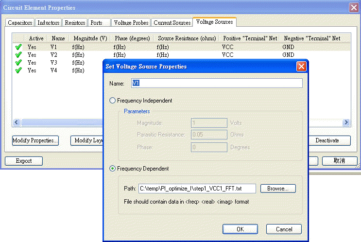
1.8.1 Export "Data Table" of U41_VCC1 from Designer as a frequency dependent source for SIwave "Voltage Source"
SIwave \ Circuit Elements \ Voltage Source
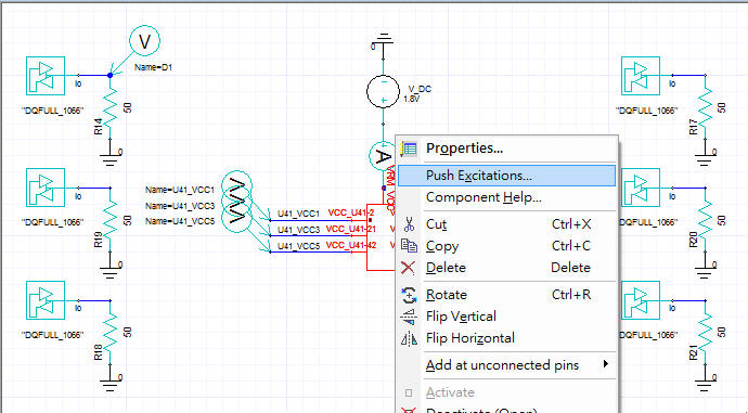
1.8.2 Push excitation
Step 1.8.1是從Designer匯出power的頻域成份,再於SIwave中引入當voltage source,這方法必須每個voltage source指定。另一方法是push excitation,可以將所有excitation成份都引入,也是官方建議的flow。
重新在Designer建一個電路直接連結SIwave:
[Project] \ [Add Model] \ [Add SIwave Model]匯入SIwave project
做完時域模擬後,即可對PCB symbol按右鍵做[Push Excitations]
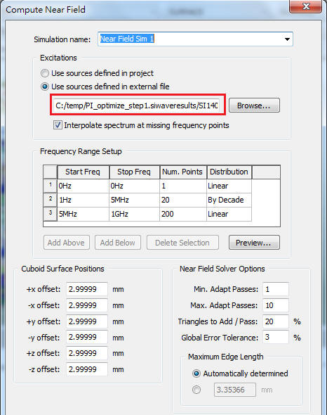
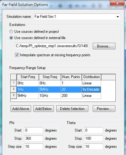
1.8.3 SIwave \ Simulation \ Compute Near Field
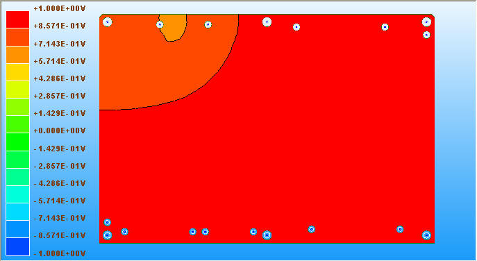
請注意,這裡的[Cuboid Surface Positions]表示SIwave計算近場的距離(118.11mils=3mm),等一下我們在在HFSS內做incident wave/data link時,建的radiation boundary大小,就依實際PCB尺寸,加上這[Cuboid Surface Positions]的offset值3mm
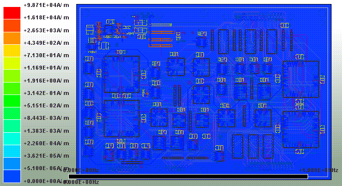
1.8.4 SIwave \ Results \ Near Field \ Near Field Sim1 \ Plot Near Fields
|E| field 0Hz ~ 1GHz
|H| field 0Hz ~ 1GHz
1.8.5 SIwave \ Simulation \ Compute Far Field
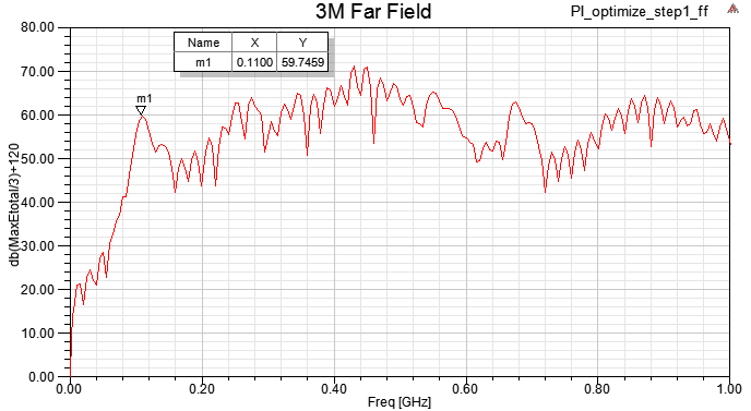
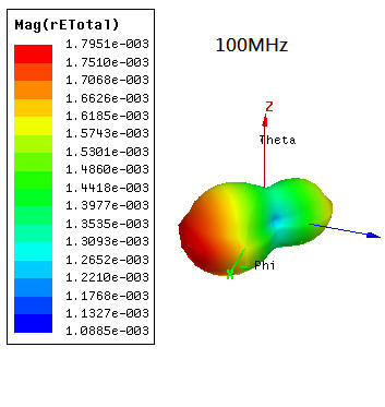
1.8.6 SIwave \ Results \ Far Field \ Far Field Sim1 \ Plot Far Fields
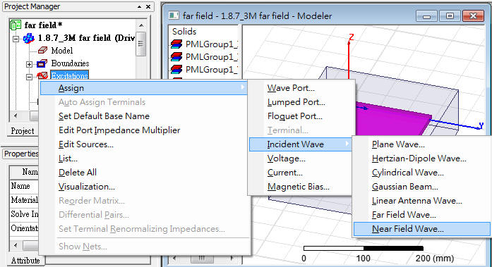
1.8.7 Create a HFSS design to simulate far field emission.
Create a virtual box (box size=PCB size + 2*near field offset) with a radiation boundary, and assign a incident wave (Incident Field or Enforce H Field) to the radiation boundary.
HFSS \ Results \ Create Emission Test Report \ Rectangular Plot
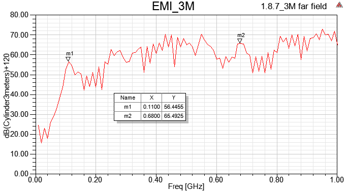
1.8.7.1 Use [Incident Field], and set the projected object as "pec"
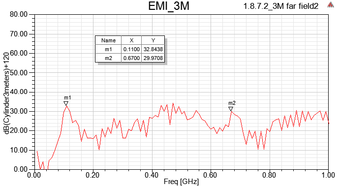
1.8.7.2 Use [Incident Field], set the projected object as "vacuum", and remove outer air box
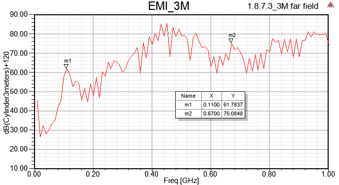
1.8.7.3 Use [Enforce H Field], and set the projected object as "pec"
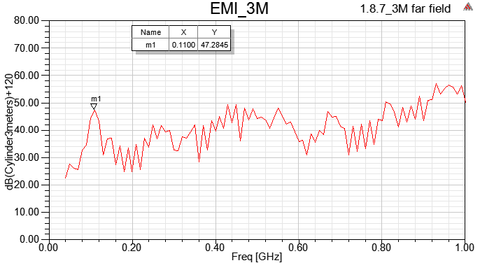
1.8.7.4 Use [Enforce H Field], and set the projected object as "vacuum"
以上四種incident wave的方式,在HFSS內得到的Emission Test Report頻點趨勢都相同,但值的大小卻不同。如果想跟FCC EMI規範比,筆者個人習慣用1.8.7.1的做法。

-
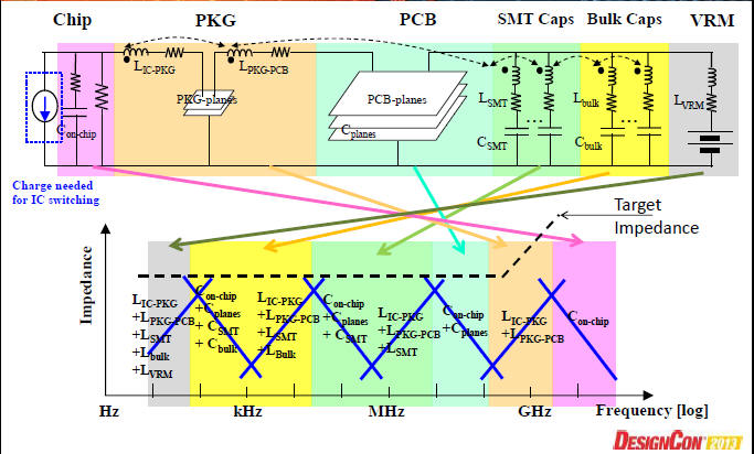
Measure Peak Current to Determine Maximum (Target) Impedance

此步驟的主要目的是為了求出target impedance.
2.1 Connect DC 1.8V to power net of DDR2 IBIS directly, and assign the same "seed" for input data pattern
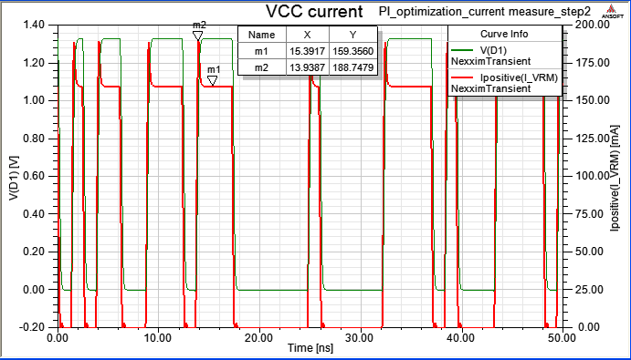
2.2 Six DDR2 full drivers totally consume 159.3mA and Ipp=188.7mA on VRM_VCC 1.8V.
The "maximum" target impedance for U41 on VCC can be designed by (1.8*10%)V/188.7mA=0.95 ohm.
Define the maximum target impedance 0.95 ohm up to 750MHz, and the design has to meet the spec.
-
Add Bulk Capacitor (100uF)
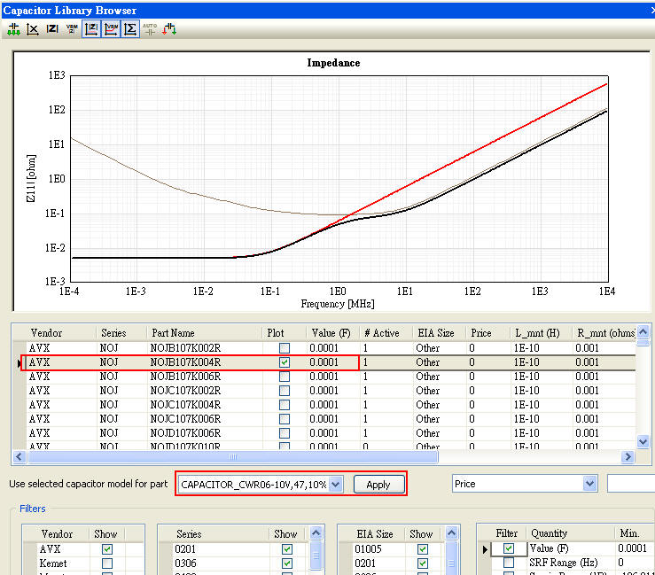
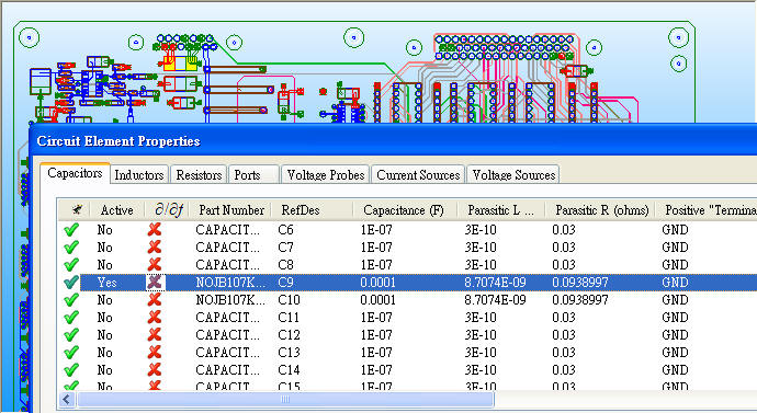
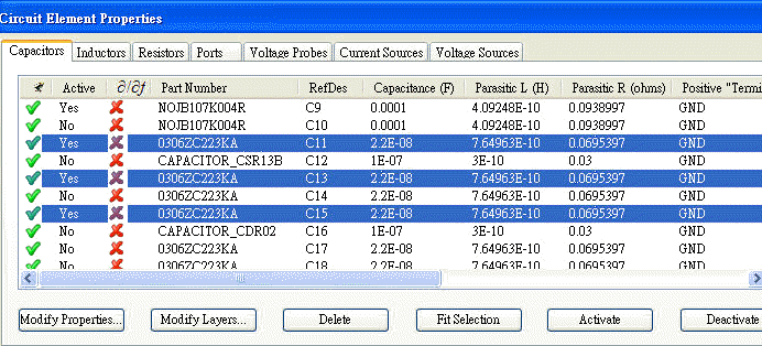
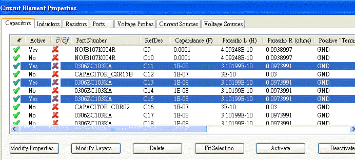
4.1 Add C9=100uF (set C9 active) with a real C model selected by SIwave \ Capacitor Library Browser
4.2 Compute SYZ-parameter again, and Z-profile as below
-
Add decoupling Capacitor (10nF)
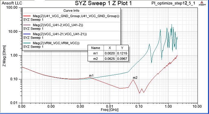
利用resonance analysis來決定如何擺放小電容以壓制寬頻的impedance
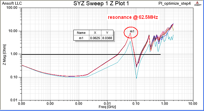
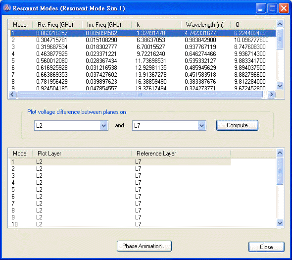
6.1 Run [Compute Resonant Mode], and check where is the area with resonance 62.5MHz between Layer2 and Layer7
6.2 Place decoupling cap. 22nF on C11、C13、C15、C60 to suppress 62.5MHz resonance
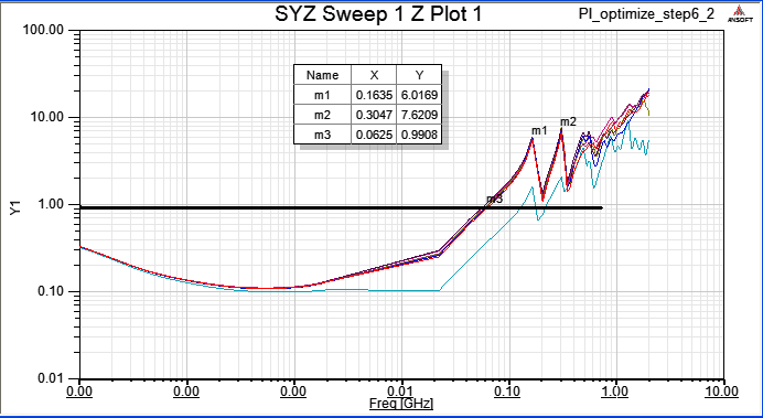
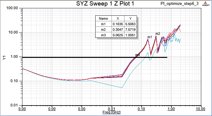
Compute SYZ-parameter again, and Z-profile as below
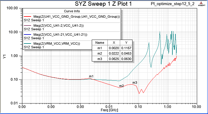
6.3 If change C11、C13、C15、C60 to 10nF
Compute SYZ-parameter again, and Z-profile as below
- Time and Frequency Domain Analysis
8.1 Place decoupling cap. 10nF on C47、C62、C63、C64 to suppress ~150MHz resonance
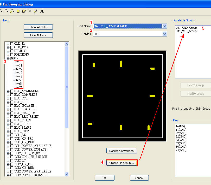
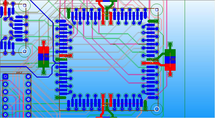
8.2 Grouping VCC and GND pins of U41 individually:Tools \ Pin Group Manager
Create VCC-GND grouping port for U41:Circuit Elements \ Generate on Components
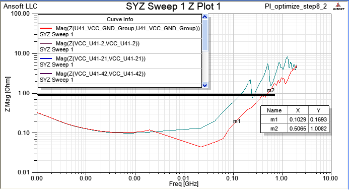
8.3 Run [Compute SYZ-parameters] again, and find out that Z-profile with a grouping port is much better than just pin ports.
-
Add HF capacitor (2.2nF+3.9nF)
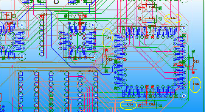
9.1 Follow up step 8.1, and place decoupling cap. 680pF on C65、C66、C67、C68 to suppress 100MHz~1GHz resonance
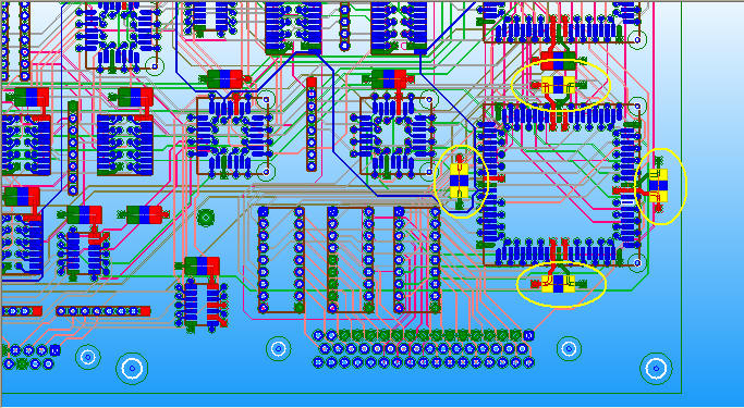
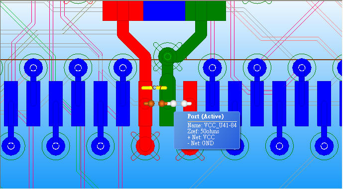
9.2 All VCC_U41-xx ports are placed on top layer, to minimize the loop inductance, rearrange the high frequency decoupling capacitors C65、C66、C67、C68 on U41 VCC and GND pins, and change to 2.2nF, just as below.
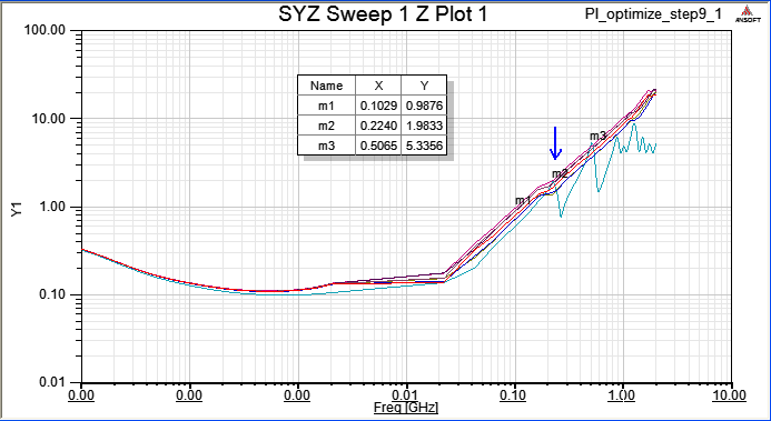
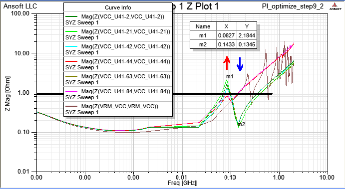
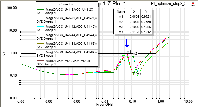
9.3 Add decoupling cap. 3.9nF on C69、C70、C71、C72 to suppress 82MHz resonance
-
Time and Frequency Domain Analysis
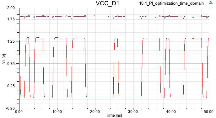
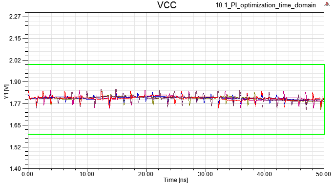
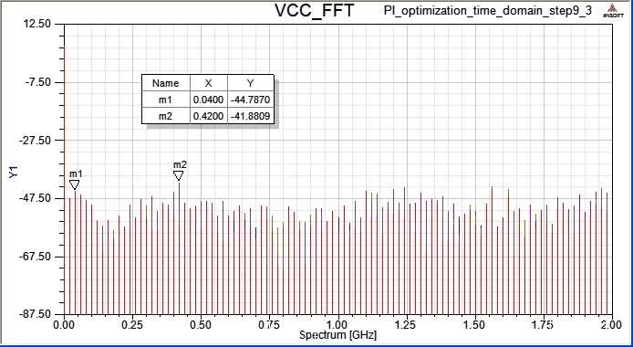
10.1
10.2
10.3
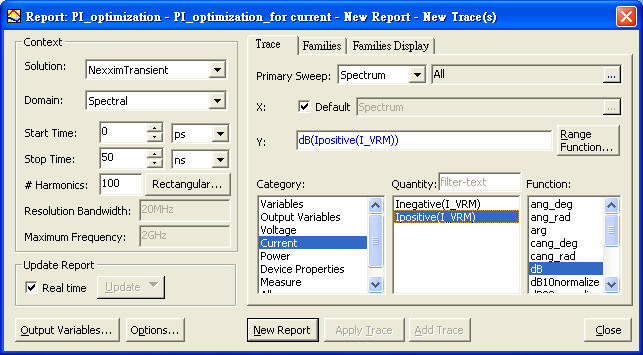
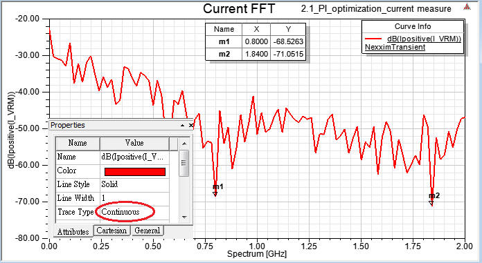
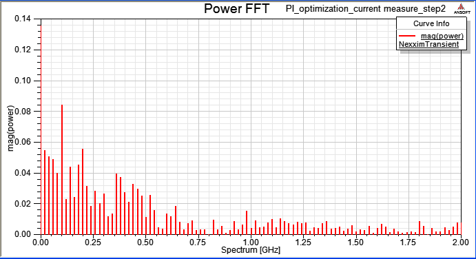
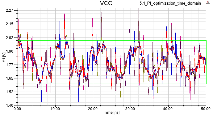
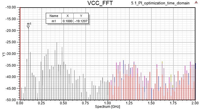
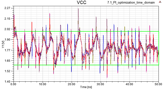
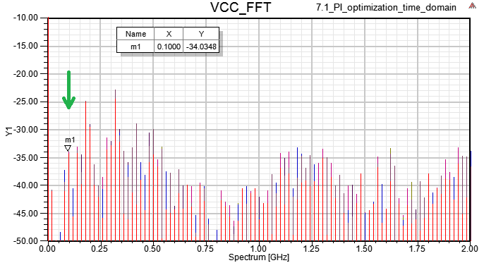
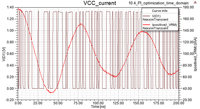
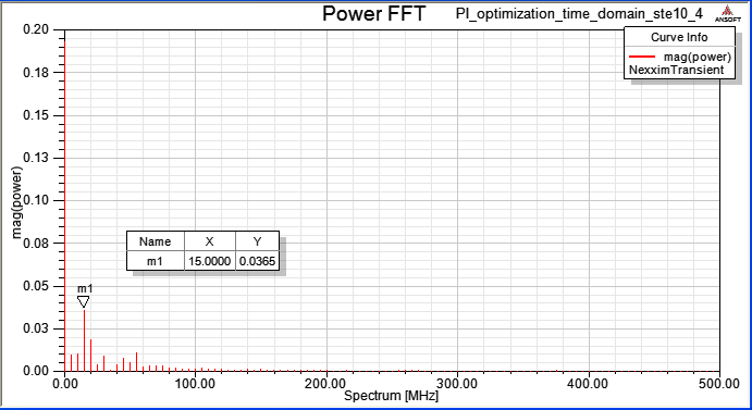
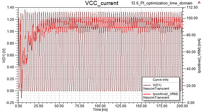
10.4 Magnitude and Spectrum of VCC current
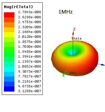
11.1 SIwave \ Results \ Near Field \ Near Field Sim1 \ Plot Near Fields
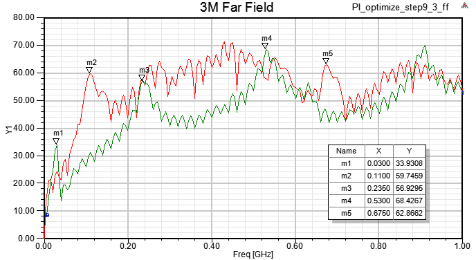
11.2 SIwave \ Results \ Far Field \ Far Field Sim1 \ Plot Far Fields
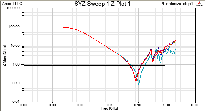
step11.2(green line)與step1.8.6(red line)相比,在500MHz以下EMI下降很多,尤其在110MHz

-
問題與討論
12.1 step1.8為何SIwave與HFSS跑出的Far Field不同?
Ans:SIwave得到的遠場結果與HFSS Emission test report不同,有以下幾個因素:
-- 本文用HFSS中Incident Wave\Near Field Wave\選SIwave,assign到HFSS的boundary,然後計算Emission Test Report。這樣做法的優點是速度快,HFSS不用去求解整個PCB真實細部結構,但缺點是引用SIwave的結果投射到HFSS內的boundary,此時被投射的box相對位置與大小、outer air box使用radiation boundary的大小(或用PML),都會導致模擬結果不同。(如果air box使用radiation boundary且設的過小,某些頻段的遠場會量到較高的值,即radiation boundary反射回來的成份)
-- 選SIwave的near field做投射,Radiation Boundary的屬性,設"Enforced Field"與"Incident Field"的profile類似,但level會有差異-- SIwave far field與HFSS內的Emission test report是不一樣的。請參閱push excitation
12.2 如何把HFSS跑出的結果,單位從dB換算成dBuV?
Ans:1V=20.log1=0 (dB) , and 1V=10^6uV=20.log10^6=120 (dBuV)
x dB = x+120 dBuVSIwave的far-field默認是1米的距離,如果要換算成3米的結果 = dB(x/3)+120
12.3 SIwave中,step1.8.5 far field plot選MaxETotal與ETotal有何差別?
Ans:"ETotal" means the maximum of the total rE-field. When calculating the maximum far field values, the distance r is factored out of the E-field. Therefore, the units for the maximum field data values are given in volts.
12.4 HFSS中,Radiation Boundary的屬性,設[Incident Field]與[Enforced Field]有何差別?
Ans:[Incident Field]是把Incident wave pattern入射於surface,其特性是absorbing boundary condition (ABC), 外面不可以再包一個ABC。如果要用[Incident Field]到internal radiation boundary,則把被投射體整個設成"pec"或移除outer ABC即可。[Enforced Field]=[Enforce H Field]則是讓Incident wave正切於surface輻射 ,boundary內是不考慮的,外面必須再包一個radiation boundary。
12.5 數百MHz以上要靠板級去耦合電容來壓impedance較不容易(ref. 1, 2),除了電容要選對、放的夠近、via的影響、放板子哪一面...,關鍵是不能讓decoupling path的loop inductance成為dominate。但大部分的板子,其實PI不用設計到如此辛苦,也都function work,那我們取VDD*10%來推算PI design spec.是否過於嚴苛?
Ans:取VDD*5%、10%,或15%來推算PI design spec.,這不是絕對,就看整個系統的design budget怎麼麼分配;PI做的差些,就吃掉一些SI的budget,或吃掉一些高低溫測式的穩定性。一般3.3V IO的數位電路,規格書會保證±10%的電壓飄移可以正常工作,但實測可能低到2.7V都沒問題。但這不意味系統工程師就可以賭IC容許10~20%電壓飄移程度下穩定動作,由其是瞬間的IR drop。
12.6 step 10.4下電容把VCC impedance降低後,雖然VCC上的Vpp降低,但VCC current會出現非週期性低頻成份?
Ans:如果driver output是random pattern,那VCC被抽的總電流會看到非周期性低頻成份,但如果driver output是clk,那VCC被抽的電流最後會穩定。
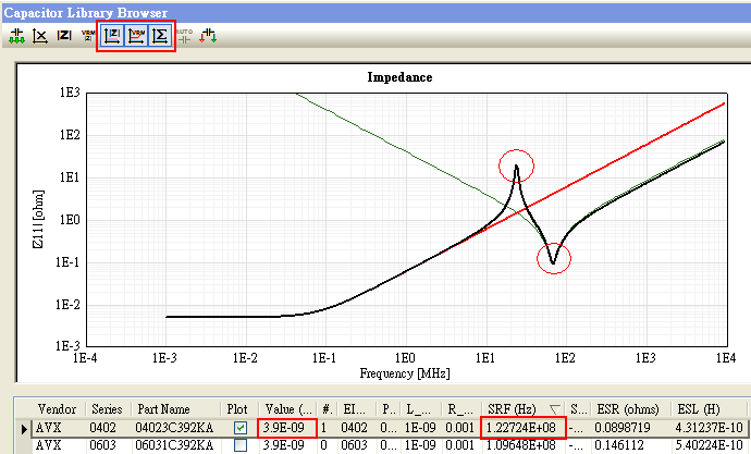
12.7 Capacitor Library Browser可選擇頻寬、ESR、ESL適合的電容,但為何Z-profile中所示的諧振點(谷點)與SRF頻點不同?
Ans:SRF所指的電容自諧振頻點,是由表列中的C value、ESR、ESL所決定,是選定電容型號後就決定的,是不能由使用者任意更改的。表列中另外還有L_mnt、R_mnt是指 把電容焊上板子,pad與歐姆阻抗所貢獻的寄生效應,這部份使用者可自行更改,並且觀察到Z-profile顯示的谷點會隨之變化;即C value、ESR、ESL、L_mnt、R_mnt共同決定了Z-profile所顯示的谷點位置。
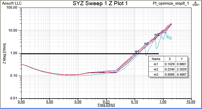
12.8 step9.3加四顆3.9nF的電容就近放在U41 pin,在100MHz新增一個拉低的頻點(谷點),但左側62MHz卻新增一個拉高的頻點(峰點)?
Ans:我們選定一個去耦合電容,是要利用其Z-profile上最低點的該頻段來壓低PDN impedance,但在該頻率的左邊,會因為與VRM output impedance的加成作用而形成一個在Z-profile上阻抗高點,如下圖所示
12.9 為何此例中,100MHz以上的PDN impedance特別難壓下來(step 9.1),必須把電容直接下在IC pin上才能看到效果(step 9.2)?
Ans:此例100MHz以上,即使選用高頻的小電容,如果不放在IC pin腳上,就看不出impedance降低的原因有二:
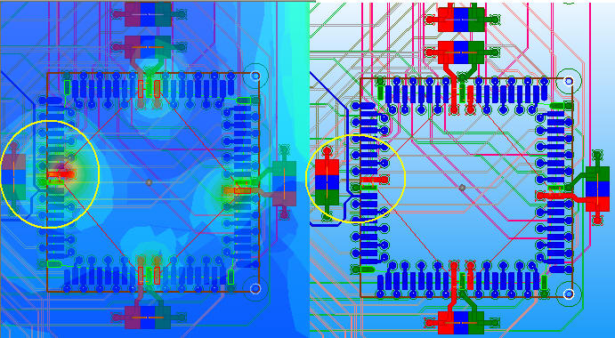
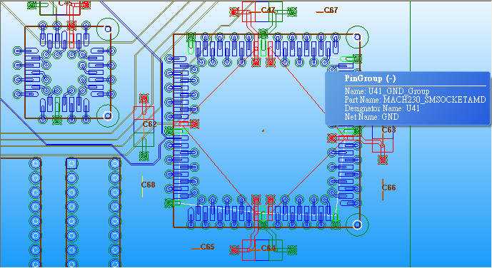
12.9.1 主因:此例的power、GND ports是by pin下的,而不是by device group,這會造成高頻所看到的loop inductance變大。可以把它想成:前者每個pin連到reference plane看到的是一個via的效應,後者看到的是多個via並聯的效應。到底哪一種設法較正確,取決於IC+封裝本的PI design是不是夠理想,如果夠理想,那用pin group的方法較正確,否則就要by pin下port才夠worse。
實務上每根VCC (GND) pin可視為近似等電位,所以我們把U41的VCC-GND ports改成以pin group的方式重新建立
Follow step 9.3 and run it again with group port
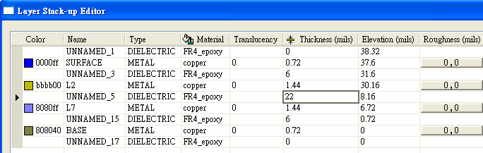
12.9.2 此例是堆疊比較特殊(較差)的八層板,layer 2是GND,layer 7是VCC。而一般PCB疊構設計不讓power、GND plane間隔太多的signal layer,因為會造成PDN impedance較大,且power、GND plane夾不出高頻buried capacitor。若把本例疊構改成一個power、GND plane相鄰的四層板
官方文件Ansoft 2008 presentation p.7,18可以看出U41有用grouping port,但p.14~16又轉成是by pin下port看到的結果。筆者以前做PI就都是用grouping port,沒碰到過問題,但也不知用[pin group]有何差別,現在終於明白。
-
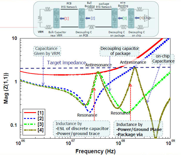
For the IC with several numbers of power/ground pins, have to use "pin group" individually.
-
The performance of decoupling capacitor depends on loop inductance.
-
Board level capacitors can reduce impedance below 400MHz, and capacitor in package or buried are for more higher frequency.
[1] Power Plane and Decoupling Optimization by Ansoft
[2] EMI drive by PI issue by Ansoft 2008
[3] H.H. Chuang, W.D. Guo, "Signal/Power Integrity Modeling of High-Speed Memory Modules Using Chip-Package-Board Coanalysis", EMC2010. (推薦)
[4] K. Shringarpure, S. Pan, "Innovative PDN Design Guidelines for Practical High Layer-Count PCBs", DesignCon2013. (推薦)
[5] Tzong-Lin Wu, "Power Integrity and EMC Design for High High-speed Circuits Packages", 2008. (推薦)