Online video
Home > ANSYS HFSS 教學 > IC EMC
The article started in 2018.10 and demonstrated IC EMC simulation with 2018.2 SIwave and HFSS. It intended to introduce the IC EMC measurement and test defined by IEC, how to do IC EMC simulation (CPM+IBIS), and how to do it in case you can't get CPM(Chip Power Model) model from IC vendor.
-- update 10.3, 2022.07.01
-
IC-EMI Measurement (IEC 61967)
-
IC-EMS Measurement (IEC 62132)
-
IC Impulse Immunity (IEC 62215)
-
IC-EMI Behavior Model (IEC 62433-2,3)
-
IC-EMI Behavior Model, I/O model (IEC 62014)
-
IC-EMS Behavior Model (IEC 62433-4,5)
-
IC Impulse Immunity Behavior Model (IEC 62433-6)
-
IC-EMI Simulation with CPM Model
9.2 Attach CPM to package in SIwave
9.3 Run Transient analysis with CPM and IBIS
9.4 Push-excitation to get far-field EMI in SIwave
9.5 All the steps above can be done by HFSS+Designer
9.6 Full System EMI consideration (IC+PKG/PCB+test environment, FE-BI)
-
IC-EMI Simulation without CPM Model
10.1 Modeling current source by time domain measurement data
-
IC-EMS Simulation with CPM+CECM Model
11.2 IC ESD (off-power) immunity test with CPM+CECM model
11.3 System ESD (on-power) immunity test with CPM+CECM and package model
-
Q&A
13.1 What if I can't get the IBIS I/O model?
13.2 What causes the different far-field EMI between HFSS and SIwave? (important)
13.3 Why 9.4.3 have not the EMI contributed by I/O toggle, but it doesn't seem better? (important)
13.4 How to plot the maximum near field by spectrum on a plane with a specified distance?
![]()
In recent years, due to the rising demand for industries such as 5G/AI/virtual currency, higher-speed and high-power IC/package design requirements are increasing at an alarming rate. For example, the most complicated package I saw two years ago was 7000 bumps, and the most complicated package seen this year is 110000 bumps (average current 350A, instantaneous maximum current 500A), which has increased the complexity by 15 times in two years. It freaks me out. For those doing SI/PI/EMI, the challenge is getting more significant and tough, and they have to find better and more efficient methods throughout the design and simulation process.
This article will introduce applicable IC EMC simulation methods based on the measurement/testing defined by IEC and makes practical discussions from these simulation results.
-
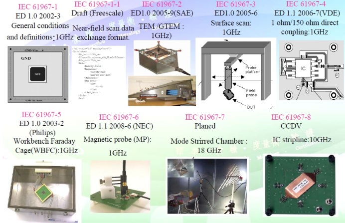
IC-EMI Measurement (IEC 61967)

The following picture is taken from the materials compiled by Professor Lin of Feng Chia University.
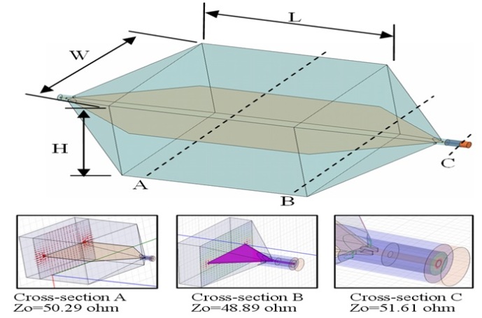
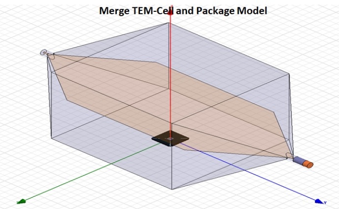
IEC 61967-1 defines a 10cmx10cm four-layer PCB with a complete reference plane. The tested IC is layouted on one side (placed in-side a IEC 61967-2 defined TEM Cell), and all traces and passive components are layouted on the other side.
IEC 61967-3 is mainly used to measure the EMI emitted from the top of IC. There are some commercial EMI scanners on the market, and the industry uses a lot (as NEC EMI scanner).
IEC 61967-6 is mainly used to measure the EMI from the trace. It can get the larger inductive amount, but the resolution of the magnetic probe for space is not good.
-
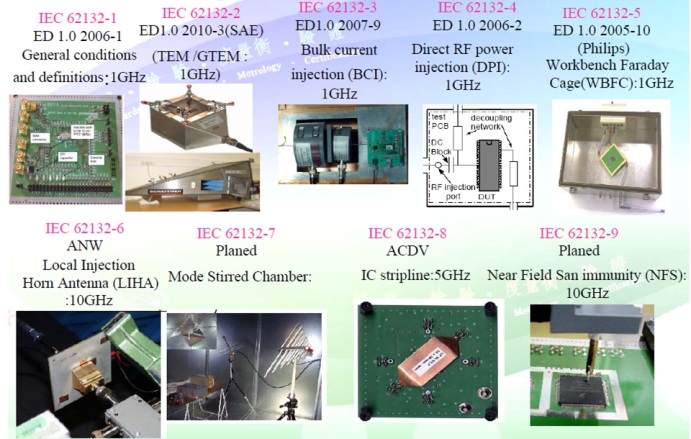
IC-EMS Measurement (IEC 62132)
The following picture is taken from the materials compiled by Professor Lin of Feng Chia University.
IEC 62132-2 and ICE 61967-2 test instruments are basically the same, except that the operating procedures are reversed. The former uses the conductor plane in the middle of the TEM-Cell to emit radiant energy to interfere with the EUT (IC), and the latter uses the conductor plane in the middle of the TEM-Cell to detect the radiated interference (EMI) emitted from the EUT (IC).
IEC 62132-3 directly injects current noise to the IC pin with current probe.
IEC 62132-6/7/8/9 is currently undecided, but in 2018, there is an IEEE paper following IEC 62132-8.[3]
-
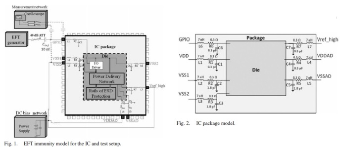
IC Impulse Immunity (IEC 62215)
IEC 62215-2 p.6 shows:Future standards will be similar to IEC 6100-4-2 /4/5 (ESD/EFT/Surge) [4][5]
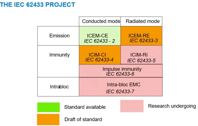
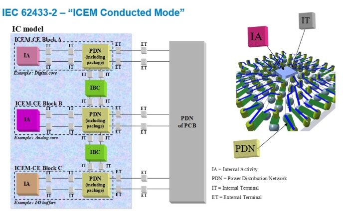
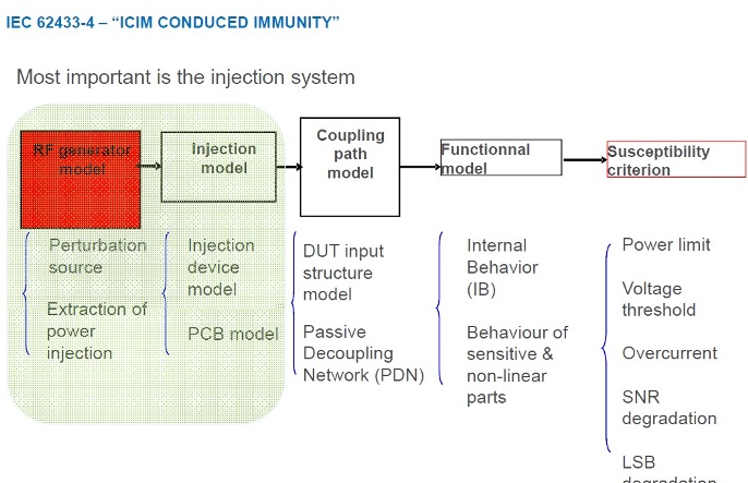
- IC-EMI Behavior Model (IEC
62433-2,3) [6][7]
IEC 62433-2 defines that the IC model must include internal activity (IA), power delivery network (PDN), and package/PCB parasitic effects.
This is actually the CPM (Chip Power Model, i.e., IC current source + IC PDN) + Package model. For a long time, this is not only the EDA manufacturer promoted, but IEC regulations also defined like this.
-
IC-EMI Behavior Model, I/O model (IEC 62014) [8]
This is the I/O behavior model, that is, the IBIS model that people who simulate SI/PI use almost every day.
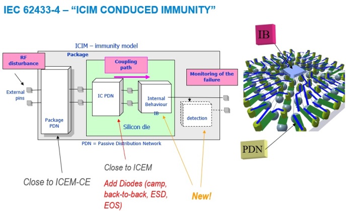
- IC-EMS Behavior Model (IEC
62433-4,5) [6][7][9]
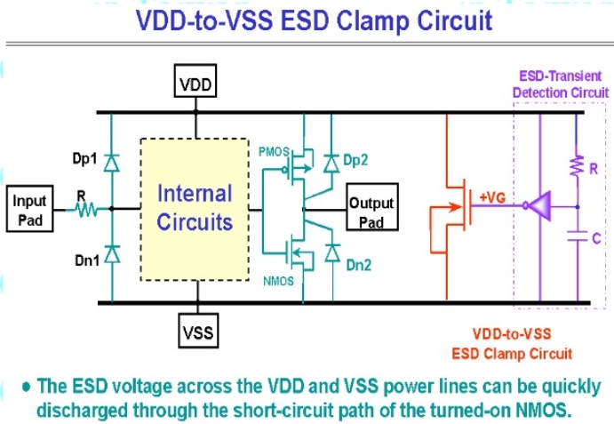
Comparing to IEC 62433-2, IEC 62433-4 adds diode/clamp/back-to-back component models. That is, in addition to IC PDN (passive RLC), consider the non-linear devices, including diode and clamp for ESD behavior in IC.
If you don't understand why the on-die diode and clamp (RC drive NMOS) are needed for ESD in IC, please refer to the NCTU Professor Ming-Dou Ker website.
In the practice of simulation, the most important thing is the generation and injection of interference sources, that is, to implement the EMS noise generator, such as ESD/EFT/Surge generator.
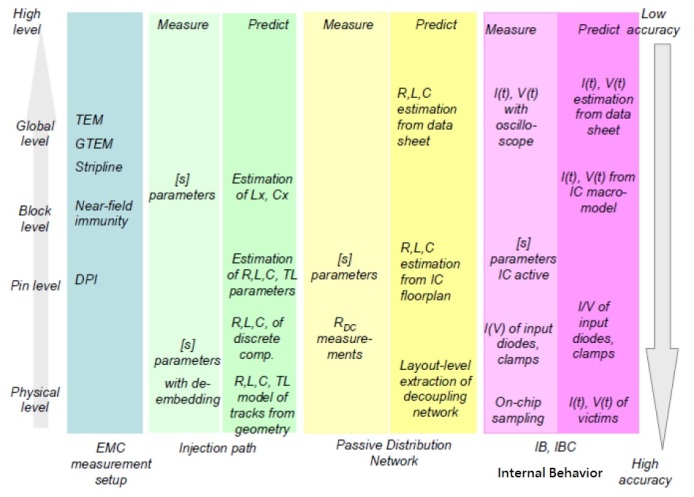
From left to right, consider the Source/Coupling Path/Receiver, the three main factors of EMC. Consider the actual physical model from bottom to top, from IC to system (through simulation or measurement).
Have you understood the description above ? After all, how does IEC suggest us to simulate IC EMC?
Don't you still understand?
Do you see it recommended using CPM (Chip Power Model) for the core model and IBIS for I/O model?
If you don't see it, try to look it back a few more times ... and you will see that ...
-
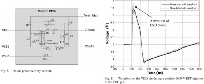
IC Impulse Immunity Behavior Model (IEC 62433-6)
Let's take a look at a 2014 IEEE paper [10].
I accidentally found the first author, Ji Zhang, who graduated from Tsinghua University in Beijing, China. After receiving a Ph.D. from Missouri University, USA, he works for CISCO and writes [11] [12], a talented guy whom I admire.
-
IC-EMI Simulation with CPM Model
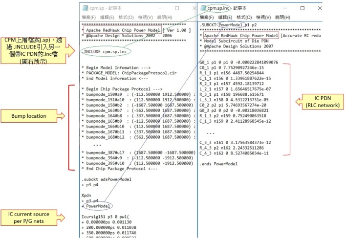
9.1 ANSYS CPM model
The ANSYS CPM model is composed of two SPICE files, .sp and .inc. The former contains the Power/Ground port to net 0 current source definition (i.e. The IA defined in IEC-62433-2), and the latter contains IC Power/Ground RLC network definition (i.e. PDN illustrated in IEC-62433-2). Each header of a file has its declaration of Apache RedHawk Chip Power Model.
Import and test your CPM model coming from IC vender first. To notice that not every CPM model is generated from ANSYS. refer to 13.5
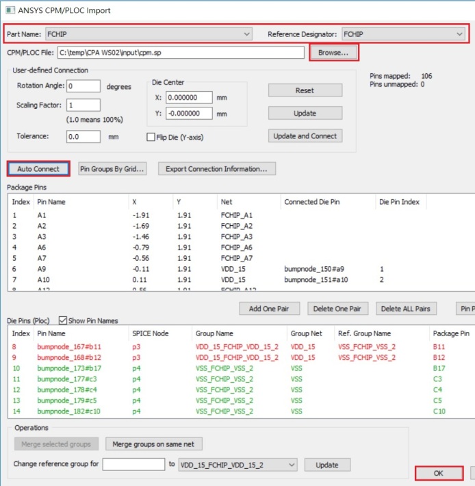
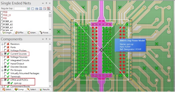
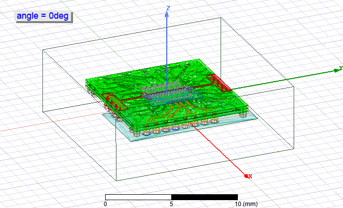
9.2 Attach CPM to package in SIwave
Attach CPM on DIE side by SIwave [Import] Tab \ [ANSYS CPM/PLOC file]
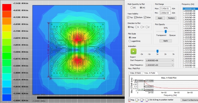
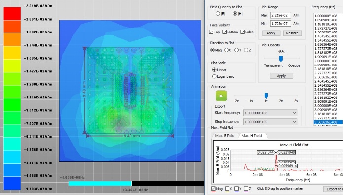
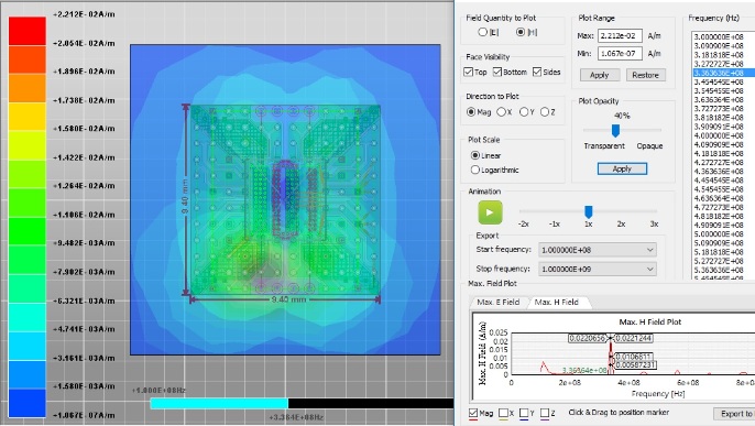
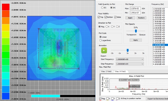
Run SIwave near-field analysis (EMI triggered by P/G current only that is defined in CPM), H-field at 100MHz
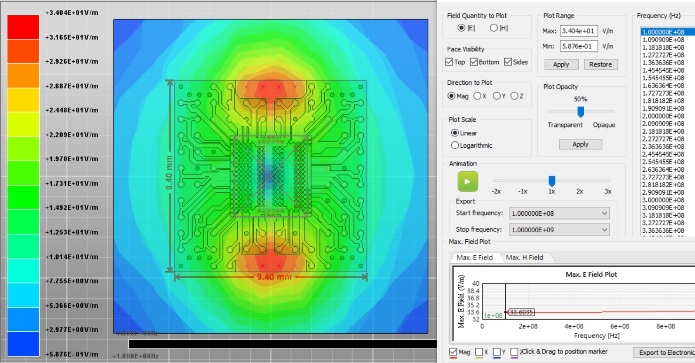
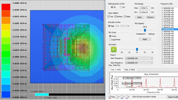
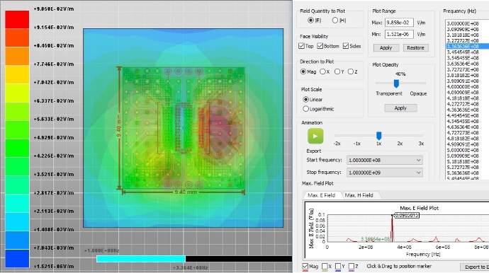
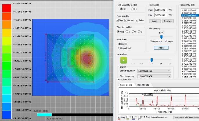
Run SIwave near-field analysis (EMI triggered by P/G current only that is defined in CPM), E-field at 100MHz
Run SIwave far-field analysis (EMI triggered by P/G current only that is defined in CPM)
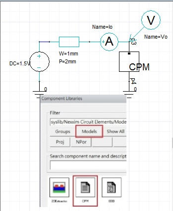
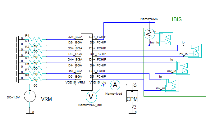
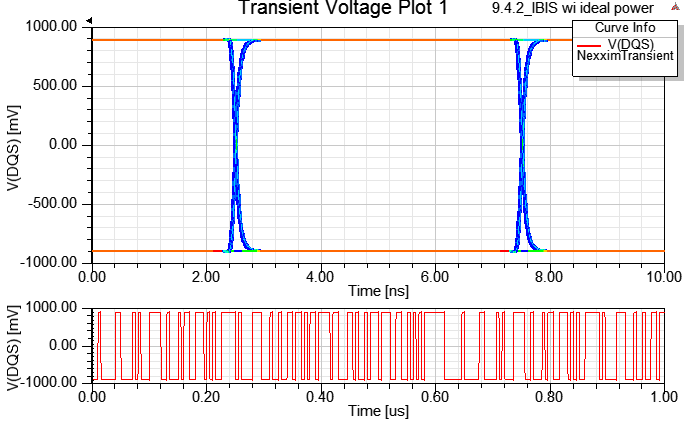
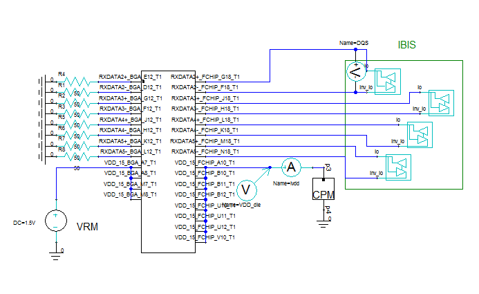
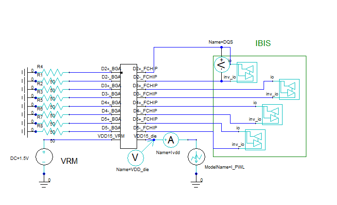
9.3 Run Transient analysis with CPM and IBIS
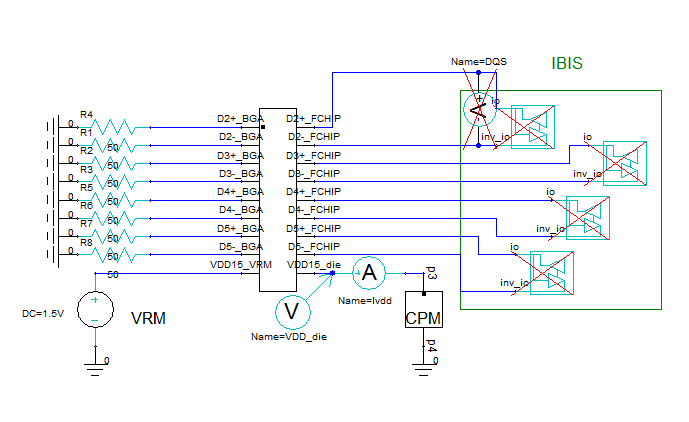
De-active the CPM and voltage/current source in SIwave first, and connect CPM, IBIS and package model in Designer as below.
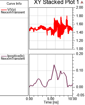
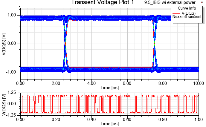
CPM + Package model + IBIS model with external power (non-ideal power 1.5V)
Please remove parasitic package parameter in IBIS, due to we have included package model extracted by SIwave here.
9.4 Push-excitation to get far-field EMI in SIwave
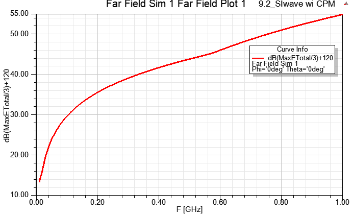
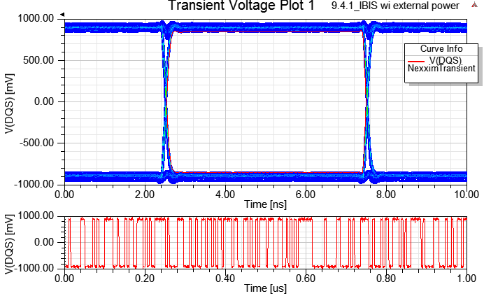
9.4.1 Run SIwave near/far-field analysis (EMI triggered by P/G current and IBIS with 5ns bit time)
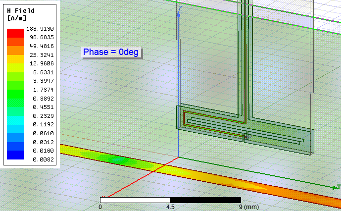
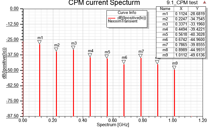
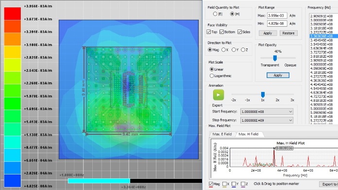
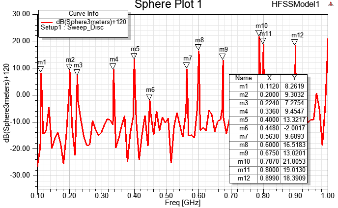
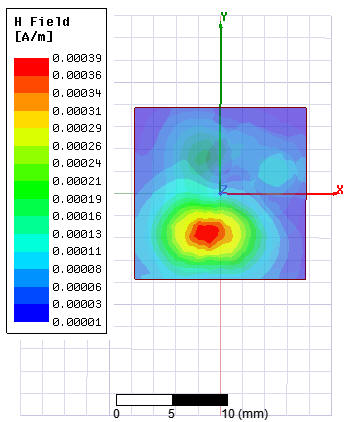
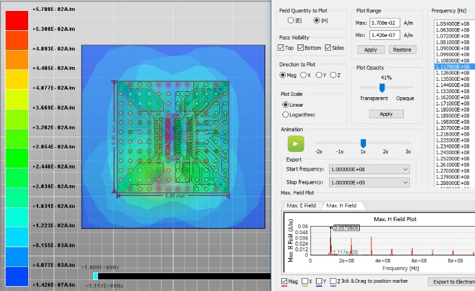
EMI triggered by P/G nets (CPM) and I/O nets (IBIS), H-field at 336MHz. (the energy of 336MHz is from CPM current)
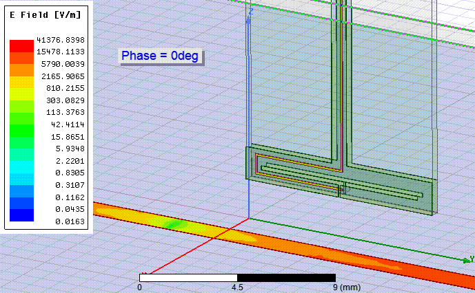
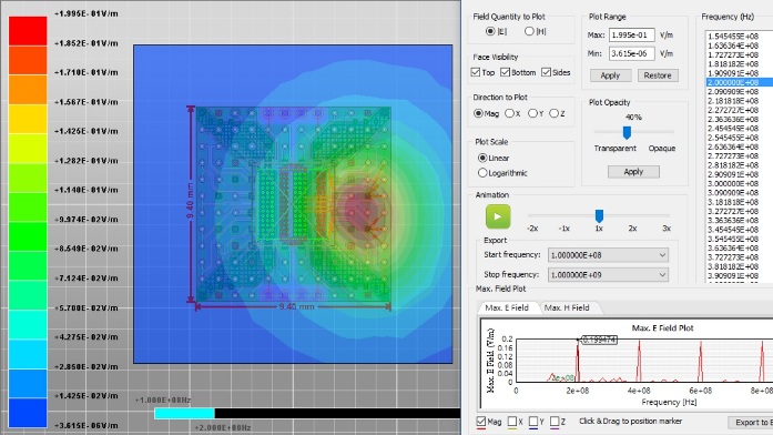
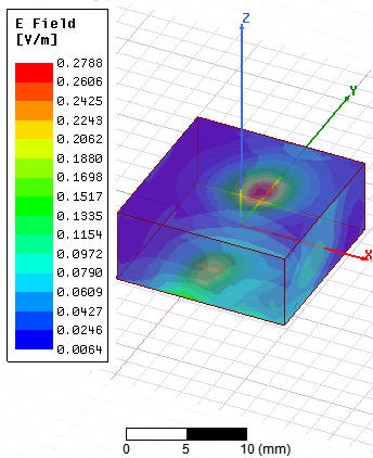
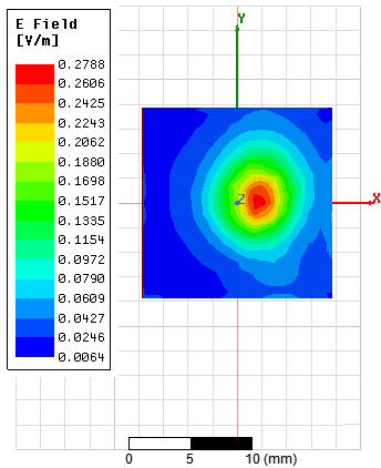
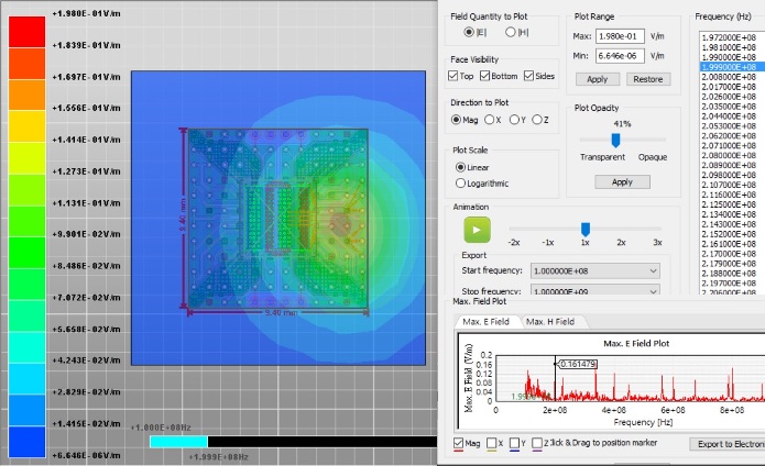
EMI triggered by P/G nets (CPM) and I/O nets (IBIS), E-field at 200MHz
The most substantial region of E field at 200/400/600/800/1000MHz is precisely the position that the four pairs of high-speed signal lines located (IBIS I/O high-low toggle with 5ns bit time).
This includes the IC CPM current (224/336/448/562/674MHz...), the impact of IBIS I/O charges and discharges on PI, and the radiation (200/400/600/800MHz...) caused by high-speed traces.
9.4.2 CPM + Package model + IBIS model with internal (ideal) power
EMI triggered by P/G nets (CPM) and I/O nets (IBIS), H-field at 336MHz
EMI triggered by P/G nets (CPM) and I/O nets (IBIS), E-field at 200MHz
This includes the IC CPM current (224/336/448/562/674MHz...) and the radiation (200/400/600/800MHz...) caused by high-speed traces but does NOT include the impact of IBIS I/O charge and discharge on PI (due to internal power for IBIS).
9.4.3 CPM + Package model + Open IBIS model
9.5 All the steps above can be done by HFSS+Designer
9.6 Full System EMI consideration (IC+PKG/PCB+test environment, FE-BI)
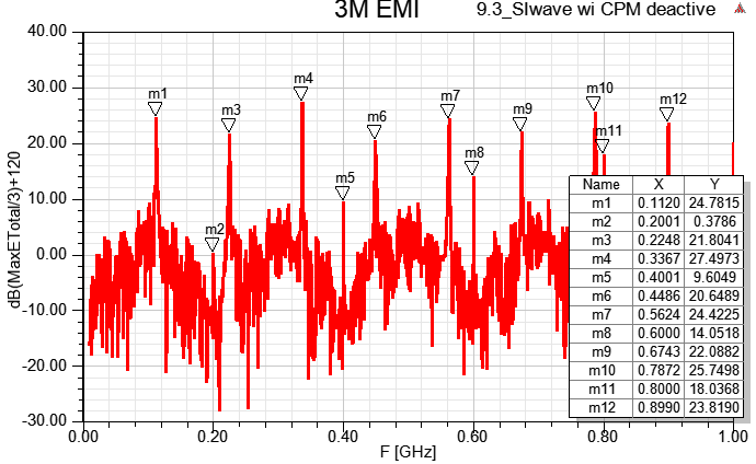
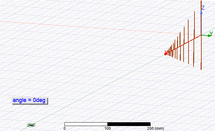
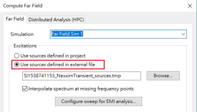
As shown above, the full-wave FEM simulation tool has been able to solve such a case with a large size ratio. To simulate IC+PCB EMI, it doesn't need to be so complicated. Just export the [Emission Test Report] by HFSS and let the software estimate |Emax|.
If you would like to put a receiving antenna in HFSS and get the same result as EMI laboratory through simulation, the first you have to perform is the wideband gain correction (post-processing) for the antenna like the laboratory did. I would not do that, and it did not be necessary.
-
IC-EMI Simulation without CPM Model
10.1 Modeling current source by time domain measurement data
For most system manufacturers without IC CPM model, you can measure the P/G current through a high-resolution current probe, and then import the measured I-T table into an I_PWL(Piecewise Linear Source) in the Designer as the IC current source.
We output the IVDD I-T table (.csv/.tab) measured by the current probe as step 9.3, and import it into the current source I_PWL in Designer. The current source now has been the result of considering the IC PDN and package parasitic RLC. Comparing the following analog circuits with 9.3, the near-field E / H and far-field EMI are almost identical.
10.2 Modeling EMI radiation source by near-field boundary
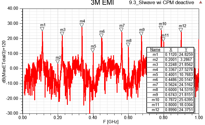
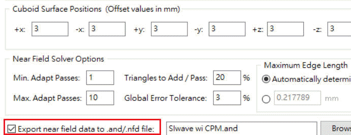
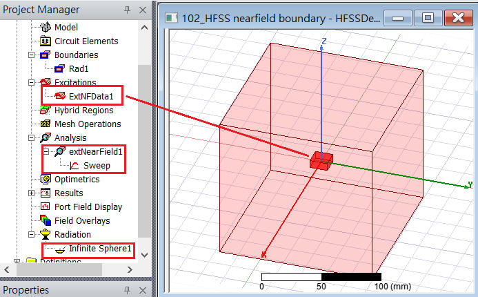
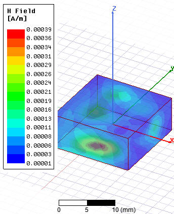
When doing [Compute Near Field] in SIwave, selecting the following [Export near field data] will output the E / H near field value (.and / .nfd) on a rectangular (hexahedral) surface at each frequency point.
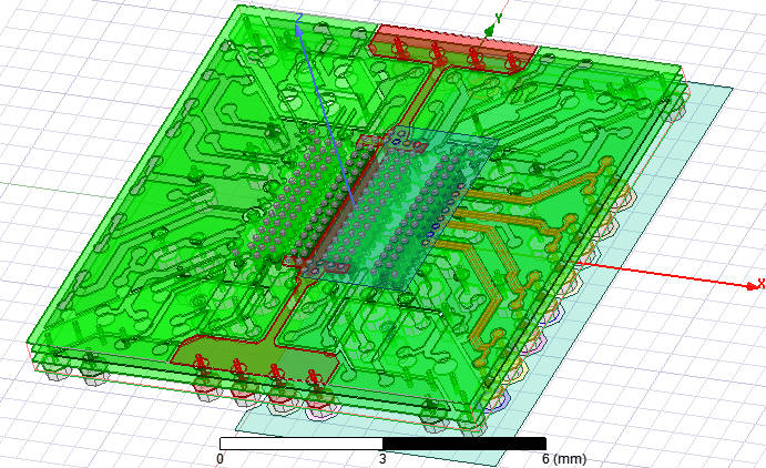
At the same coordinate position of HFSS, draw a rectangular box of the same size. Assign Excitation \ Linked Field \ Near Field \ Create External Data Design (*.and), and assign .and/.nfd near field definition output by SIwave to this rectangle box, and then you can do far-filed analysis in HFSS and output 3m EMI far-field results.
336MHz H-Field
200MHz E-Field
From the simulation above, we know, the system users can reproduce the IC EMI behavior (the EMI frequency points are entirely consistent), as long as the IC venders can provide the IC near-field E/H model (.and/.nfd exported from the software tool). Even the CPM, IBIS, and package model are lack.
10.3 Reconstruction EMI source by measurement
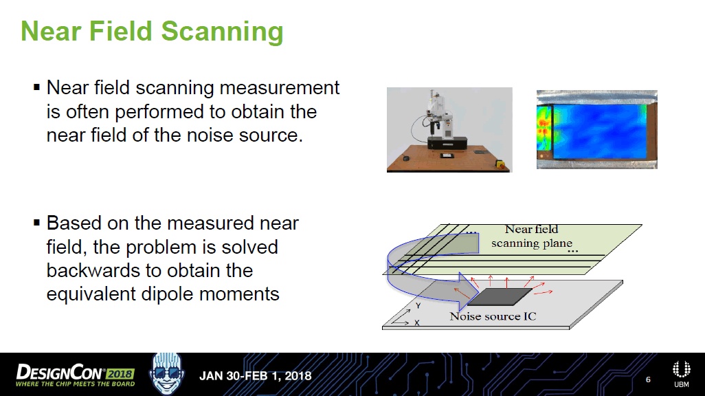
Without knowing the behavior of the IC, how to establish the EMI model of the IC through the information obtained by the near-field scanning, that is, "IC radiation source reconstruction"?
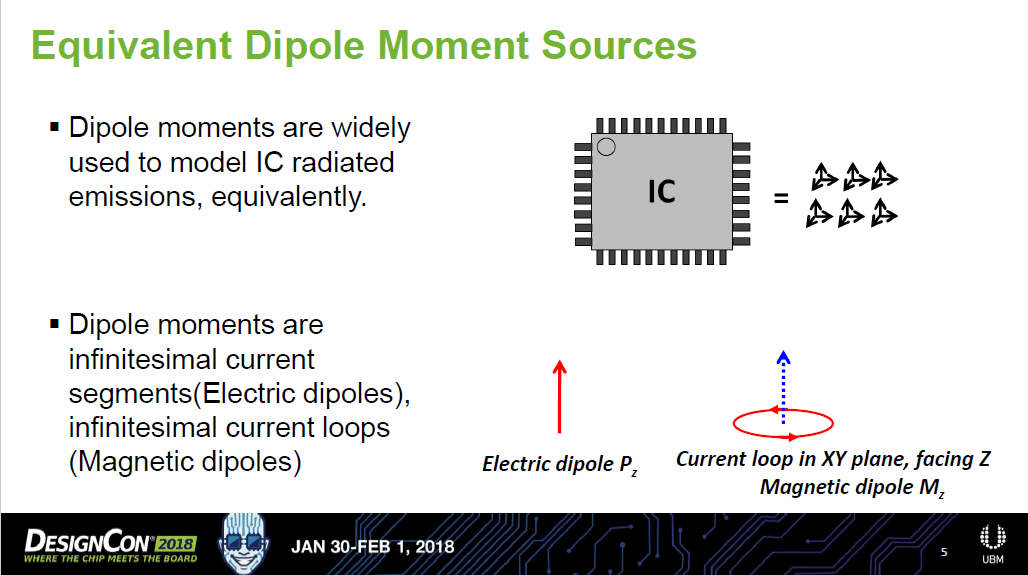
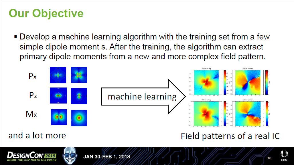
The concept is very intuitive: it uses some small electric field sources (electric dipole, current segments) and magnetic field sources (current loops) to synthesize the effect of the IC radiation field through an appropriate position configuration. [12]
How to develop a set of algorithms to find the best configuration of electric and magnetic field sources, which is closest to the actual IC near/far-field radiation behavior? Artificial intelligence/machine learning may be the answer.
"Source Reconstruction for IC Radiated Emissions", in recent years, academic circles have been discussing it, but it has not yet reached the level of commercialization.
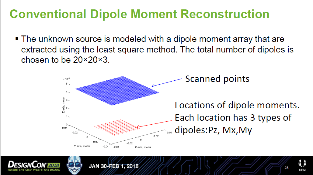
Since the the E/H near-field from EMI scanner does not contain phase information, only 2D E/H-filed with 1mm distance above the IC is not enough to restore the IC EMI source. At least two near-field information at different plane heights are required. [13]
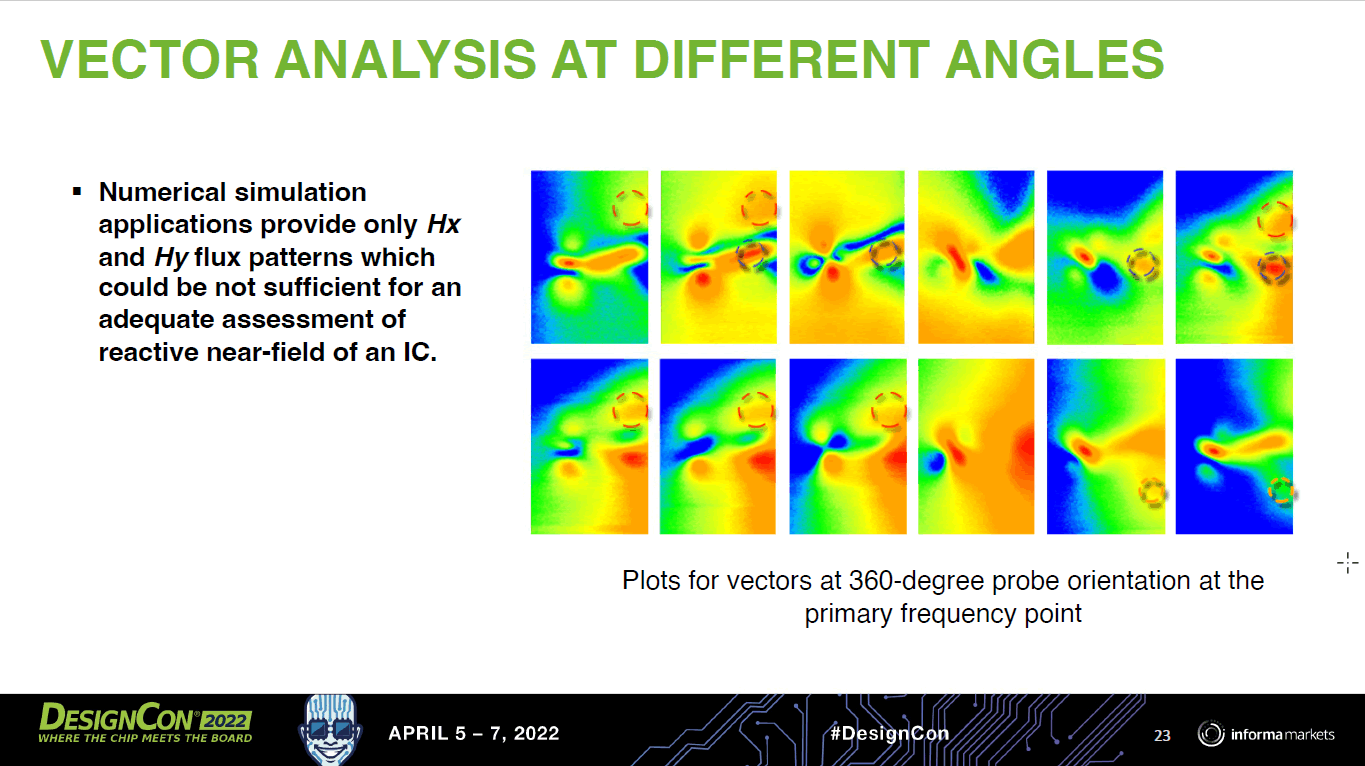
The CEO of APREL (Testing Solution Comp.) think that only Hx and Hy can NOT be sufficient to model the behavior of IC EMI in DesignCon 2022 [15].
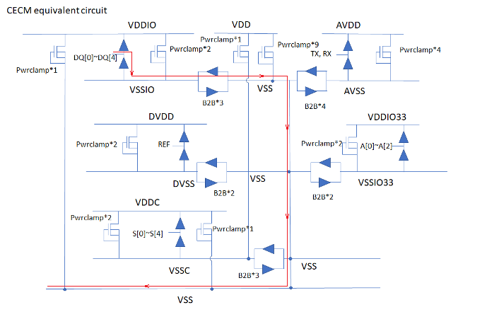
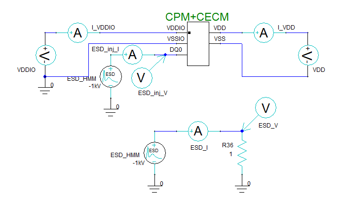
- IC-EMS Simulation with CPM+CECM Model
That is, [12][13][14] such "IC radiation source reconstruction" technology may be feasible to evaluate the far field caused by IC, but it is not good enough to find out the EMI problems and solutions of IC inside, the latter requires a more refined model. However, the near-field measurement technology of electromagnetic field is trade-off between the measurement sensitivity and spatial resolution. As shown in the magnetic field probe of IEC 61967-6 of this article.
In addition, "IC radiation source reconstruction" has the same limitations as the method introduced in 10.2 of this article. It cannot reflect when the same IC is placed on a board with different grounding conditions (different system external current return conditions), the EMI radiation of this IC. is different.
To solve the above two bottlenecks, the current best practice is: CPM (IC current+PDN) + SPICE/IBIS (IO model) + Package model.
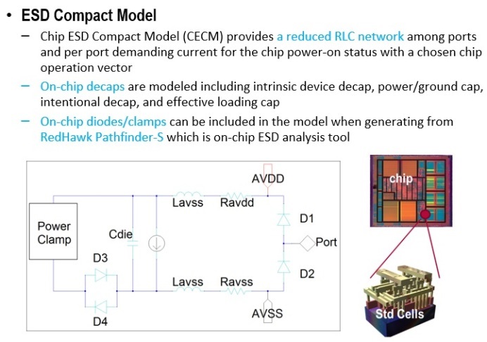
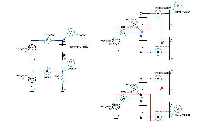
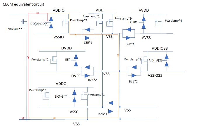
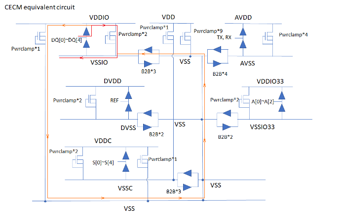
11.1 CECM test
The ESD component (Power clamp/Diode) model used in the 11.1 and 11.2 CECM was a simple behavior model described by a defined I-V curve. The conduction behavior of the component is the turn-on/forward voltage (Vf=0.51V) plus the IR drop contributed from Ron=0.01-ohm, while a 0.0001-ohm short circuit directly represents the b2b diode. The advantage is that this way is easy to observe some underlying phenomena.
The behavior of a real ESD protection component works as a good open-circuit (the P/G terminals isolated) in normal times (steady-state). It works as a low-impedance/short-circuit behavior when ESD noise occurs. The simple behavior model can only present the characteristics of the ESD protection element when it is on, but not reflect the open-circuit characteristics when there is no ESD noise. Therefore, I would suggest using the transistor level model (SPICE) instead of the behavior model (I-V curve), as in 11.3.
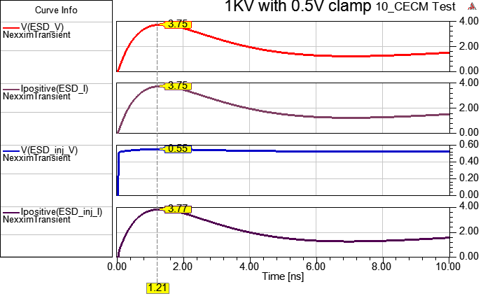
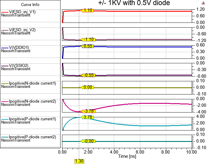
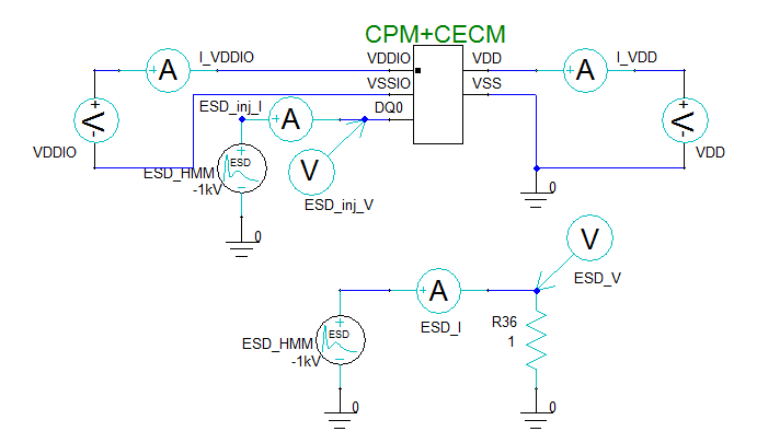
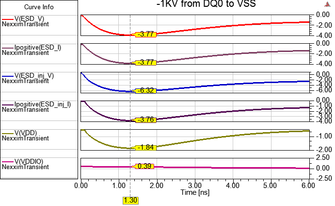
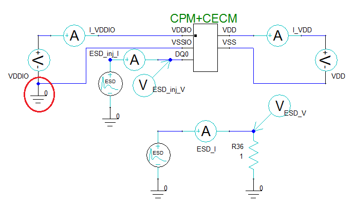
The peak current injected by 1KV ESD, no matter the load is 1 ohm or CECM model, is around 3.76A.
The voltage peak induced by +1KV ESD injection at IO terminal is ESD_inj_V1 = (0.51+3.78*0.01) + (0.51+3.78*0.01) = 1.096V as shown in the red line above.
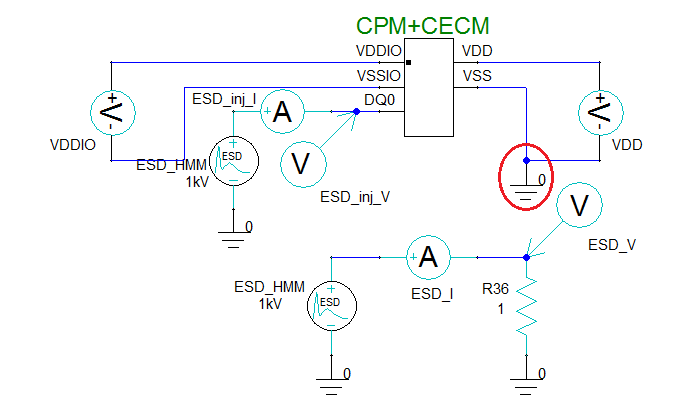
11.2 IC ESD (off-power) immunity test with CPM+CECM model
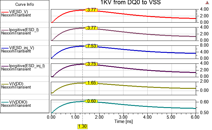
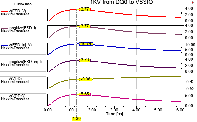
11.2.1 ESD 1KV discharge from DQ0 to VSS
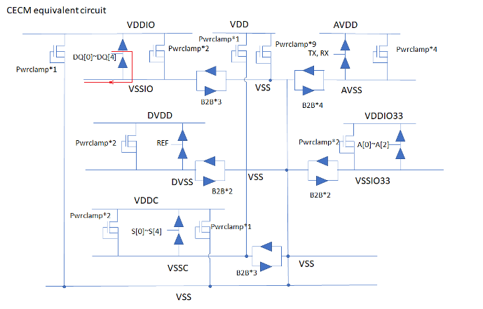
Because the voltage of VDDIO-VSSIO is 0.5~0.6V, we know that clamp between VDDIO-VSSIO is active, and the orange discharge path is a turn-on.
Why is the ESD_inj_V voltage on the DQ0 pin not limited to 0.51+0.51=1.02V, but 7.53V?
Ans : I used the transistor level model to do this example and get the same result. It seems that the IC PDN contributes ohm-level impedance at the DQ0 pin.
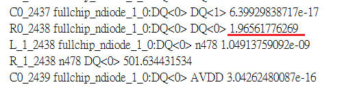
The suspects are as follows: DQ0 down (n-diode) is in series with a 1.96-ohm resistors, and up (p-diode) is in series with a 0.61-ohm resistors.
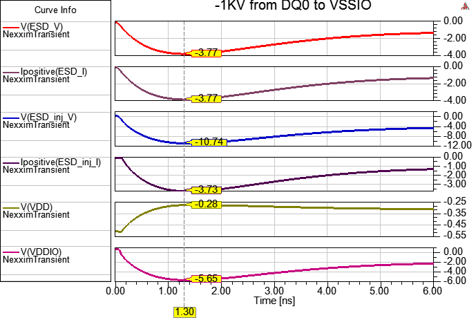
11.2.2 ESD -1KV discharge from DQ0 to VSS
11.2.3 ESD 1KV discharge from DQ0 to VSSIO
11.2.4 ESD -1KV discharge from DQ0 to VSSIO
Ans : Except for the known R0_2438=1.96 ohm resistor in series at DQ0 down (n-diode), the n-diode is connected to VSSIO with a large resistor R0_2486 in series as well. Similarly, if we change these two resistors to a smaller value, you can get smaller ESD_inj_V.
11.3 System ESD (on-power) immunity test with CPM+CECM and package model
To simulate with CPM model and package design (.mcm/.sip) is the proposed methodology for IC EMC simulation.
2.5 EM solver (SIwave) can compute EMI very fast and consistent to 3D EM solver (HFSS). (if the case with completed reference plane)
The frequency sweep setting of EMI analysis (far-field computing) is very important.
-
Q&A
13.1 What if I can't get the IBIS I/O model?
Ans:It is recommended to visit Micron/Altera website to download the DDR2/3/4 or the USB/Ethernet I/O model of corresponded speed or use the software built-in pattern source (V_PRBS/EYESOURCE/AMISOURCE) to be similar.
There are also some mature commercial IBIS generators (as SPISim), which can generate an IBIS model by inputting simple system specifications or SPICE models. (ANSYS merges SPISim in 2020)
It is not a good idea to measure the rising and falling waveforms of I/O and then manually edit the IBIS I/O model by yourself with reverse engineering. The main reason is that the measured waveform data is usually with package and PCB parasites. Most people are not only unfamiliar with the condition defined for rising and falling waveforms in IBIS, but other information required. It may take a long time for you to make an IBIS I/O model that is inaccurate or even cannot pass the grammar check.
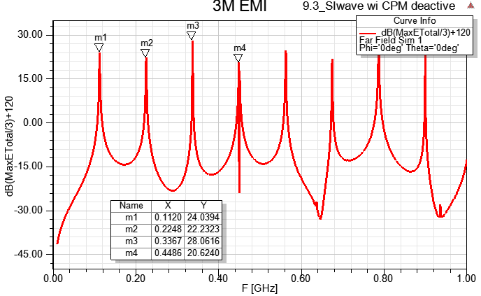
13.2 What causes the different far-field EMI between HFSS and SIwave?
Ans:
First, compare the far-field EMI results of 9.4.1 and 10.2. The main difference is the technology of calculating far-field is different. The former relies on SIwave and the latter relies on HFSS. The EMI values at the low-frequency 112/200/224MHz solved by SIwave are significantly higher than those solved by HFSS (10~15dB), and the rest are a little higher (5dB).
Then comparing the far-field EMI results of 9.4.1 and 9.5, these two solution conditions are different in terms of the far-field technology, the entire PCB extraction, and port methods. For the EMI brought by digital signal (high-speed wiring), SIwave solves pretty well (comparing to HFSS), but for the EMI brought by the P/G plane, the SIwave solution gets a higher value (worse). Nevertheless, refer to the EMI we did in 2016 between EMI SIwave and HFSS, SIwave in this example has been closer to HFSS.
13.3 Why 9.4.3 have not the EMI contributed by I/O toggle, but it doesn't seem better?
Ans:In 9.4.1/9.4.3, the far-field EMI at 112/224/336/448/562/674MH is not caused by the IBIS I/O toggle (200/400/600/800MHz), but by the IC P/G current defined in CPM, which is radiated by the P/G plane (as 9.1 CPM current spectrum show).
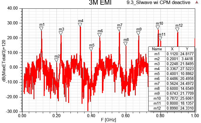
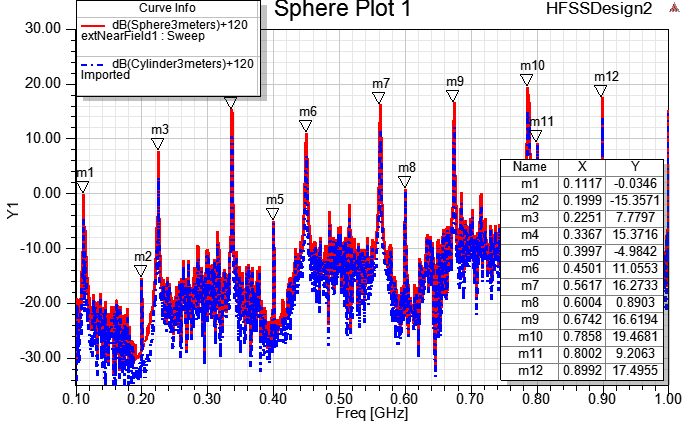
In this example, the near-field H clearly sees the only 336MHz outperforming, but the far-field shows that 112/224/336/448/562/674MH frequencies all of them are very strong. Why?
-- The near field shown in SIwave in this article is obtained by sweeping 0~1G with 101 frequency points. If we increase the sweep frequency density from 100 to 1001 points, the near field H of 9.4.1 will become as follows
Now we see the near-field H shows the 112MHz is the strongest frequency point. Its harmonic 112/224/336/448/562/674MHz... decreases rapidly after 400MHz, but the far-field look like all within 1G almost equal, why?
-- In practice, we often encounter the strongest frequency point in the near field, which is NOT necessarily the strongest in the far field.
13.4 How to plot the maximum near field by spectrum on a plane with a specified distance?
Ans:
First plot the E/H field at a specified distance (for example, 3mm above the measured object), and use Field Calculation to define a variable for the largest near field value on the plane, and then sweep frequency to plot the variable. Please refer to video for details.
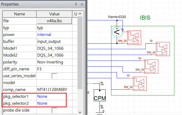
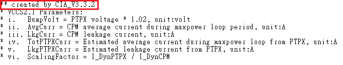
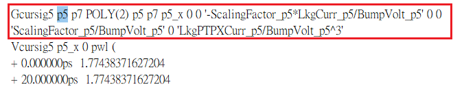
13.5 Why does sometimes a CPM include not only a current source in .inc , but also a voltage source and other items?
Ans:In addition to ANSYS and Cadence, there is a third EDA software company that can provide IC CPM model.
The following CPM model is not made by ANSYS. You have the right to blame, but please find the right person responsible.
13.6 Why is the near/far-field done with SIwave in 9.2 completely different from the one done with Designer+SIwave in 9.4.3?
Ans:The conditions of 9.2 and 9.4.3 are the same, the only source of EMI excitation is the current source defined in CPM.
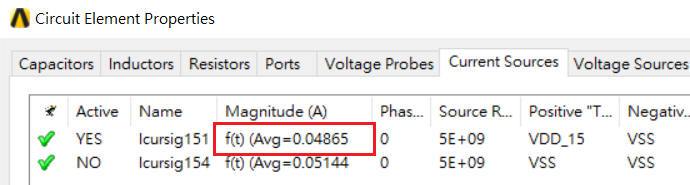
However, the EMI source in 9.2 is the current source that is automatically generated when SIwave imports CPM directly, and is with SIwave's far-field solution technology (process cross section), where the current source is "averaged" (avg).
The EMI source in 9.4.3 is the current source automatically generated by Designer pushing excitation back to SIwave. This current source is the real electrical response with considering the board, which is more accurate. Therefore, this simulation method is recommended.
13.7 As step10.2, can we input the E/H(real, imag) data scanned by the EMI scanner on the IC surface in HFSS as an IC EMI model?
Ans:No
EMI scanner can only obtain the E/H near-field information of one surface (without phase), instead of a 3D E/H near-field boundary condition composed of six surfaces, which is not enough to determine the entire radiation behavior in space. If you want to do this, at least the upper and lower E/H near-field boundary conditions are required. [13]
If you are interested in 3D near-field modeling approach for EMI, please refer to [14].
13.8 Why is the IC EMC regulation IEC62433-2 defined early ago, but the industry still rarely sees the CPM model? (Only large IC design companies have it, system manufacturers can't get it)
Ans:CPM describes the characteristics of IC power consumption, and embedded de-coupling capacitors.
These two items are the key points for the IC competitiveness, so IC design houses would not release them unless necessary, and system companies and ODM generally can not get them. However, starting from this year, due to the promotion of ADAS/AI/Bitcoin/5G application, design challenges (high speed/high power consumption) have increased quickly, companies upstream in the industry chain (as packaging and testing plants) may have the opportunity to get CPM from IC vender to make sure or speed up the development schedule of the board-level to meet the system SI/PI design requirements.
[1] IC-EMC Homepage , Software IC-EMC
[2] Generic IC EMC Test Specification - ZVEI
[3] Michele Perotti, "A Test Structure for the EMC Characterization of Small Integrated Circuits", IEEE Trans. on Instrum. Meas., vol. 67, no. 6, June 2018.
[4] Introducing IC Immunity Test, such as ESD and Latch-up
[5] IEC 62215, https://webstore.iec.ch/preview/info_iec62215-2%7Bed1.0%7Den.pdf
[6] IEC 62433, http://www.ee.cityu.edu.hk/~emc/20130502P1.pdf
[7] EMC of ICs Model (good)
[8] IEC 62014, https://www.sis.se/api/document/preview/554616/
[9] "INTRODUCING ICIM-CPI TO MODEL THE IC IMMUNITY TO CONDUCTED PULSES", EMC Europ 2017
[10] Ji Zhang, Jayong Koo, "Modeling Injection of Electrical Fast Transients Into Power and IO Pins of ICs", IEEE Trans. on Electromagn. Compat., vol. 56, no. 6, Dec. 2014.
[11] Ji Zhang, "Determining Equivalent Dipoles Using a Hybrid Source-Reconstruction Method for Characterizing Emissions From Integrated Circuits", IEEE Trans. on Electromagn. Compat., vol. 59, no. 2, Apr. 2017.
[12] Qiaolei Huang, "Machine Learning Based Source Reconstruction for RF Desensitization Analysis", DesignCon 2018.
Jun Fan, "Accurate and Fast RFI Prediction Based on Dipole Moment Sources and Reciprocity", DesignCon 2018.
[13] Ji Zhang and Jun Fan, "Source Reconstruction for IC Radiated Emissions Based on Magnitude-Only Near-Field Scanning", IEEE Trans. on Electromagn. Compat., vol. 59, no. 2, Apr. 2017.
[14] Hanen Shall, "A 3-D Near-Field Modeling Approach for Electromagnetic Interference Prediction", IEEE Trans. on Electromagn. Compat., vol. 56, no. 1, Feb. 2014.
[15] Stuart Nicol, "Magnetic Near-field Evaluation Methodology for Integrated Circuit In-package Coupling Assessment", DesignCon 2022.