線上影音
Home > ANSYS SIwave教學> EMI Analysis> (far-field and near-field) using push excitation
-
SIwave 2018.2+Designer 2018.2 using push excitation
1.2 Dynamic Link SIwave model in Designer
1.3 Push Excitation from Designer
-
HFSS 2018.2+Designer 2018.2 using push excitation
-
SIwave(near field)+Designer using push excitation+HFSS(incident wave)
3.1 Create a box in HFSS, and assign it as "PEC" material
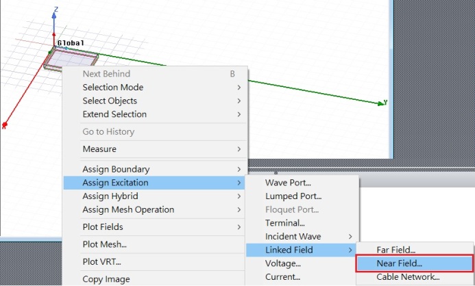
3.2 Assign an incident wave from SIwave as an excitation source
3.3 Set the radiation boundary of the box as [Incident Field] or [Enforced E\H Field]
-
問題與討論
4.2 step 1.4.2與2.1中,ETotal是什麼?
4.3 為何SIwave跑出的遠場結果與HFSS不同? (重要)
4.4 為何step1.4.3中,plot遠場強度必須/3+120? (重要)
4.6 Regular far field與Emission test report的差異在哪裡?
4.7 [Max Harmonics]與[Max. Frequency]之間是甚麼關係?
4.8 如何取得從Designer push excitation後的excited source file?
4.9 為何讀者step1.4.2自行跑出的場型,可能與本文所示不同? (重要)
4.10 分析遠場EMI的問題頻點,對應要看近場E還是H的熱點? (重要)
4.11 為何step3.3中,投射incident wave的物體要設成"PEC" material?
4.12 使用SIwave+HFSS data link (incident wave)時,如何處理PCB與機殼接地的系統级EMI模擬? (重要)
4.13 使用SIwave+HFSS data link做EMI模擬時,SIwave內near-field box size取的大小對far-filed結果有沒有影響? (重要)
-
Reference
![]()
-
SIwave 2018.2+Designer 2018.2 using push excitation
1.1 SYZ compute in SIwave
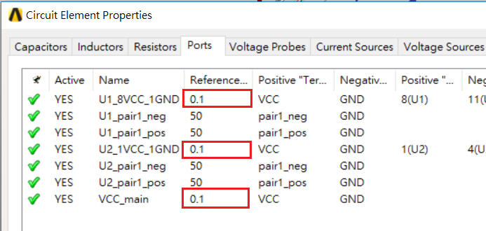
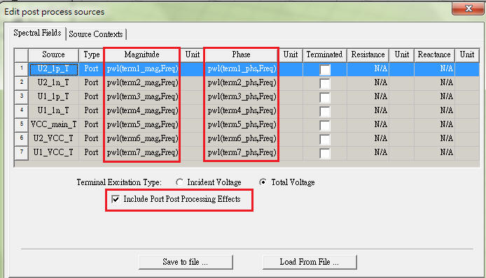
Select the critical nets/traces, and set ports for them.
Also set ports for the power/ground pin of the device used.
以本例來說,ANSYS官方範例power/ground port Zo (reference port impedance)是設50 ohm,但也有早期的官方範例對power/ground port是設0.1 ohm的。
筆者建議power/ground port的impedance設0.1 ohm,因為reference port impedance雖然對YZ沒影響,但對S參數有時會有影響。
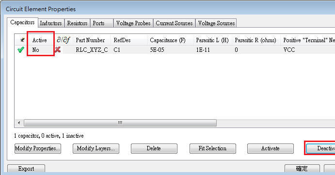
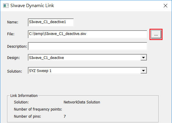
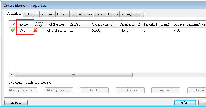
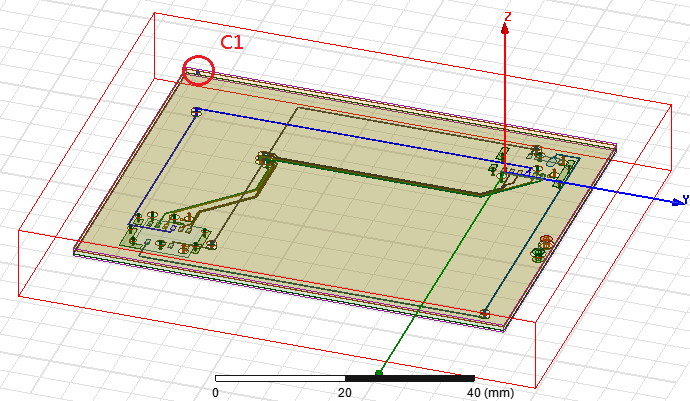
De-active capacitor C1 (50uF) at the first.
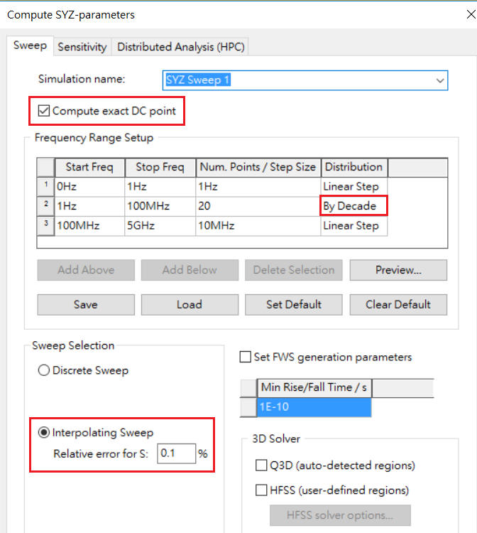
1.1.1 Set Simulation Options and compute SYZ
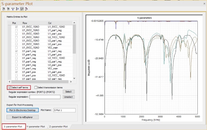
1.1.2 Then you can check the S-parameter simulation result as below
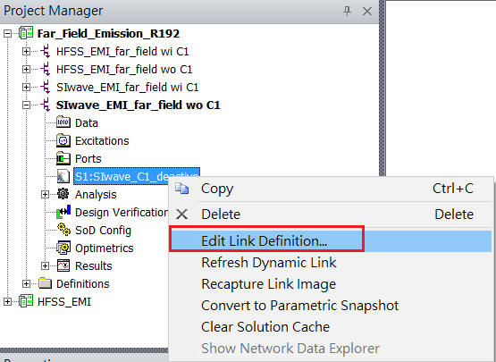
1.2 Dynamic Link SIwave model in Designer
[Circuit] \ [Add Subcircuit] \ [Add SIwave Link]
From R16, you can "drag and drop" a SIwave file into schematic window directly to link SIwave in Designer.
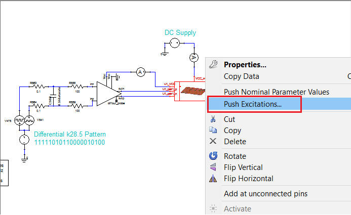
1.3 Push Excitation from Designer
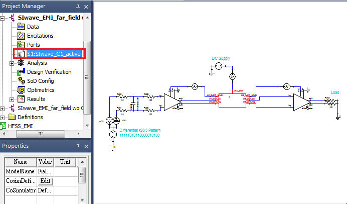
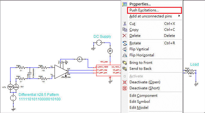
1.3.1 Drag the "SIwave model" from [Project Management] window, and [Edit Symbol] by right-click.
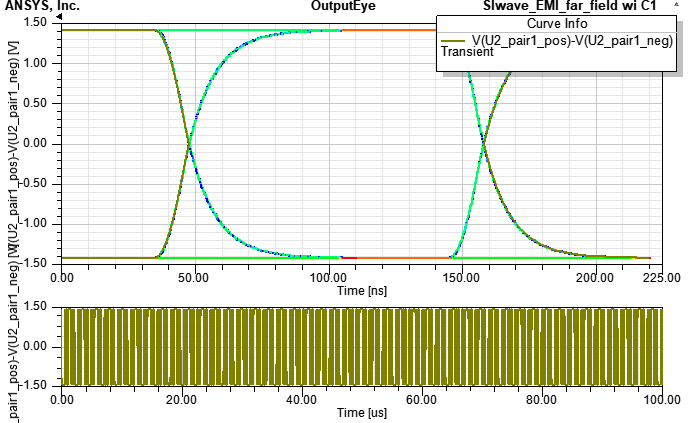
Draw a schematic to drive the SIwave model, it includes IO buffers, source pattern, DC voltage source, termination etc.
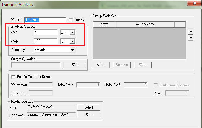
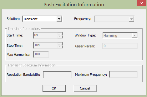
1.3.2 Set Transient Analysis, and run analysis first.
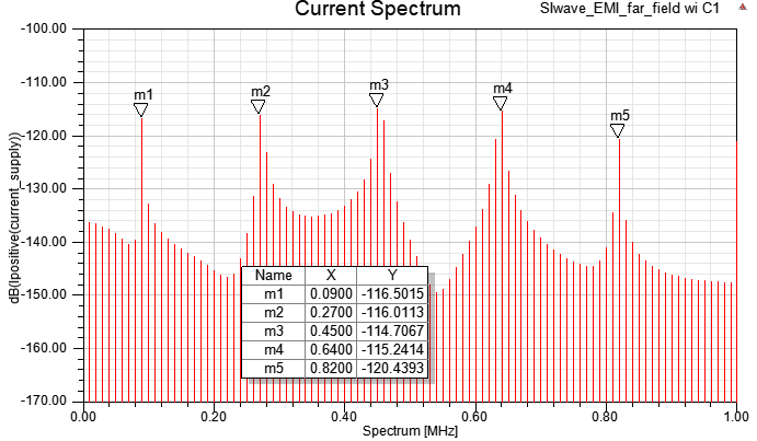
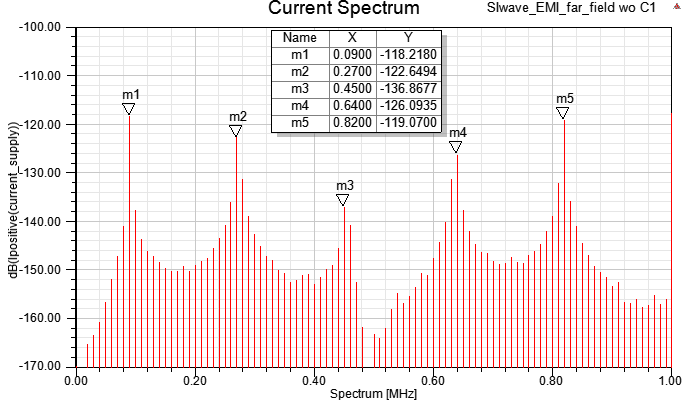
1.3.3 Review the spectrum of current (EMI concern)
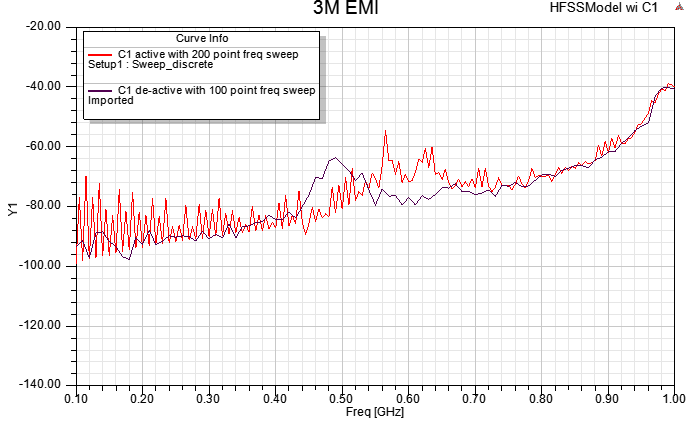
C1 active
C1 de-active
1.3.4 Then you can right-click the SIwave model symbol, select [Push Excitation] to SIwave
必須執行完Transient Analysis後,push excitation才可作用。
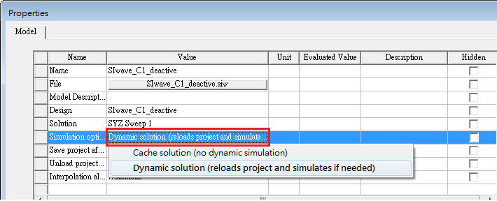
如果以SIwave dynamic link to Designer,做Push Excitation時,(SIwave 6.0起) 上圖FFT轉換window是無法設定的
如果以HFF dynamic link to Designer,做Push Excitation時,上圖FFT轉換window則是可設定的
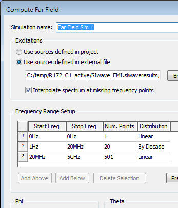
1.4 Compute far-field and plot the result in SIwave
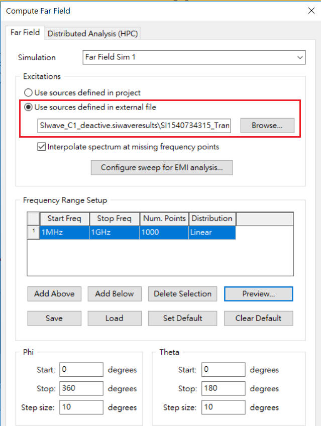
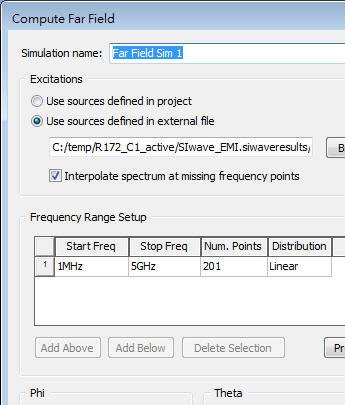
1.4.1 [Simulation] \ [SIwave] \ [Compute Far Field]
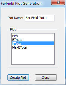
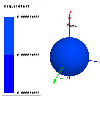
1.4.2 [Results] \ [SIwave] \ [Far Field] \ [Far Field Sim 1] \ [Plot Far Fields] with selecting [ETotal]
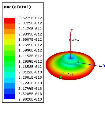
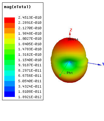
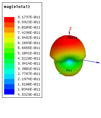
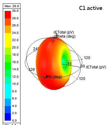
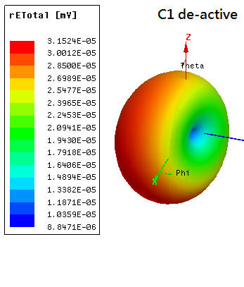
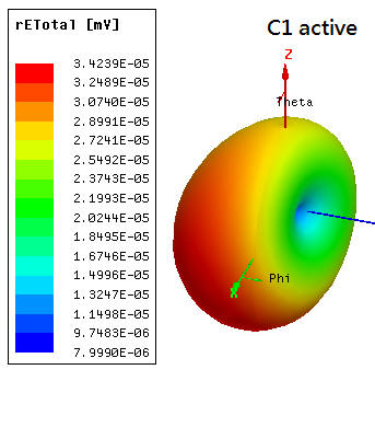
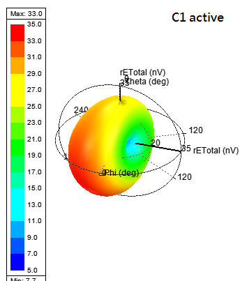
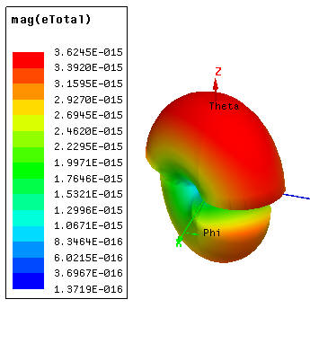
跑出的3D場型圖at 90MHz 。左圖是板級電容C1 (50uF) de-active,右圖是C1 active 。
R17.2 result
R19.2 result (Y座標無法顯示太小的值,這 似乎是在新版本UI顯示上的問題)
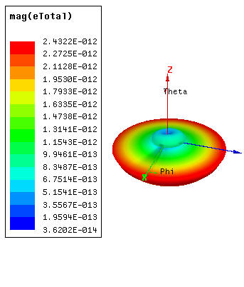
跑出的3D場型圖at 1GHz 。左圖是板級電容C1 de-active,右圖是C1 active。
R17.2 result
R19.2 result (Y座標無法顯示太小的值,這 似乎是在新版本UI顯示上的問題)
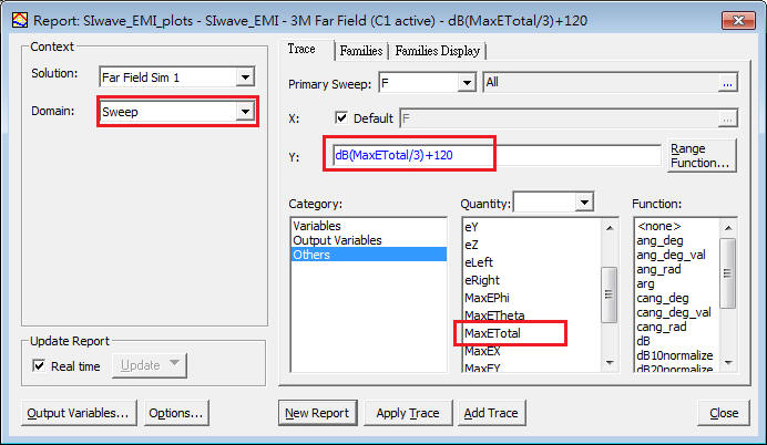
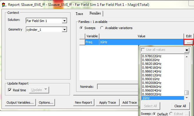
1.4.3 [Results] \ [SIwave] \ [Far Field] \ [Far Field Sim 1] \ [Plot Far Fields] with selecting [MaxETotal]
SIwave的far field report (MaxETotal)與HFSS的Emission Test Report雖然都是算|Max E|,但前者與極座標角度(Phi,Thera)相關,後者則是仿實際的EMI測試標準取最大值。故HFSS取[cylinder]是有意義的,但SIwave則不需要。所以在 新版(R17) SIwave的UI,plot far field不再出現需要指定[cylinder]的字樣。
1.4.4 SIwave遠場結果
R17.2 result (1M~1G取1000點)
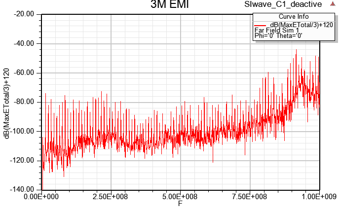
上圖所示是SIwave R17.2跑出的結果。(R17.0跑出的結果有問題,請更新至R17.2以後版本就可以得到上圖結果)
R19.2 result (1M~1G取1000點)
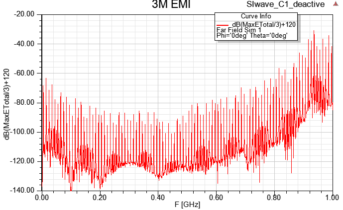
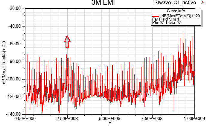
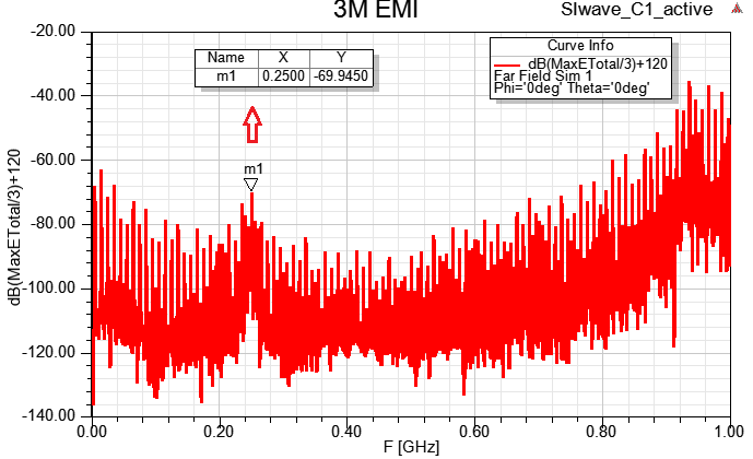
1.4.5 若把此例的板級電容C1 (50uF)在SIwave內打開(active)
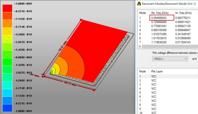
SIwave重解一次,Designer眼圖重跑,重做一次push excitation,重解Far Field的結果如下所示:此時可以看到:在250MHz略升高。而這頻點正好是做SIwave resonance mode分析可以看到的板子第一共振頻點
R17.2 result
R19.2 result (1M~1G取1000點)
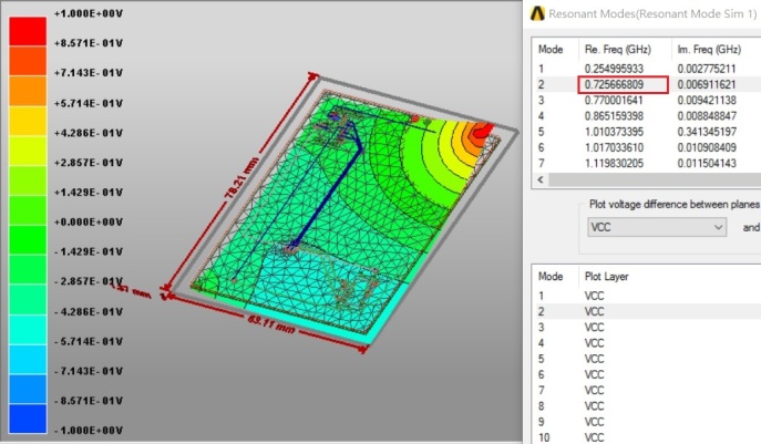
C1 active, R19.2 resonance mode result (R19.2計算的第一共振點與R17.2相同,但多了2~4三個頻點)
1.5 Compute near-field and plot the result in SIwave
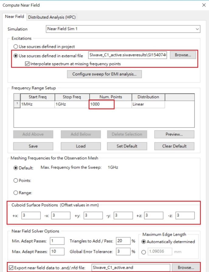
1.5.1 [Simulation] \ [SIwave] \ [Compute Near Field]
1.5.2 [Results] \ [SIwave] \ [Near Field] \ [Near Field Sim 1] \ [Plot Fields]
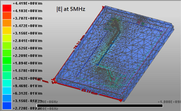
R19.2 result (1M~1G取1000點)
[Compute Near Field]求解時間,明顯比[Compute Far Field]多,因為near field求解會對近場的空間佈網格。
-
HFSS 2018.2+Designer 2018.2 using push excitation
2.1 HFSS Far-Field
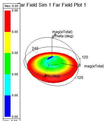
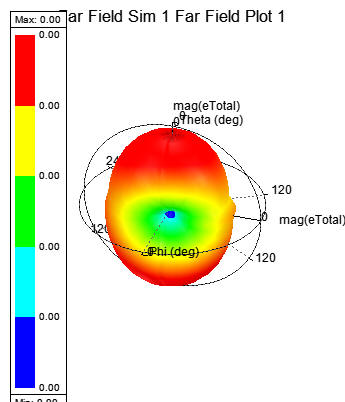
跑出的90MHz場型圖 (Far-Field 3D Polar Plot)
R19.2 result
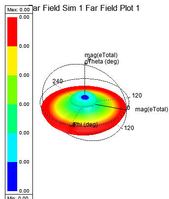
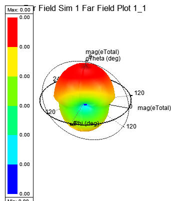
跑出的1GHz場型圖 (Far-Field 3D Polar Plot)
R17.2 result
R19.2 result
2.2 HFSS Emission Test Report
After push-excitation in Designer, you can find each ports in HFSS has been assigned an piecewise linear source (frequency domain)
HFSS的求解收斂度必須足夠,且frequency sweep設定必須正確(三段式掃頻,且內插誤差夠小),否則model可能會non-causal or non-passive,導致Designer時域內眼圖跑不出來 。
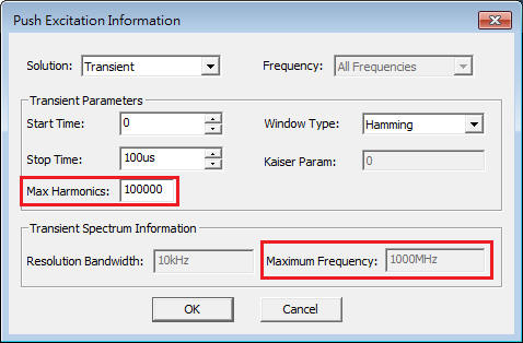
必須注意:從Designer對HFSS做push excitation時,FFT轉換的設定視窗如下,請注意Max. Frequency必須到1G,否則整個EMI準位會不對。
-
SIwave(near field)+Designer using push excitation+HFSS(incident wave)
Follow 1.4.5, C1 active
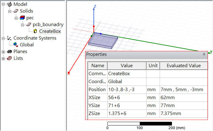
3.1 Create a box in HFSS
過去在執行此步驟時,必須打開SIwave檔案,量PCB所在位置的座標,再上下左右各延伸3mm的距離推算近場邊界的確切位置,有點麻煩。R19.x軟體的操作變簡單,只要在步驟1.5.1從SIwave export .and/.nfd file,在.and檔案的檔頭即有此near-field boundary的位置與尺寸資訊。
3.2 Assign an incident wave from SIwave near field result as an excitation source
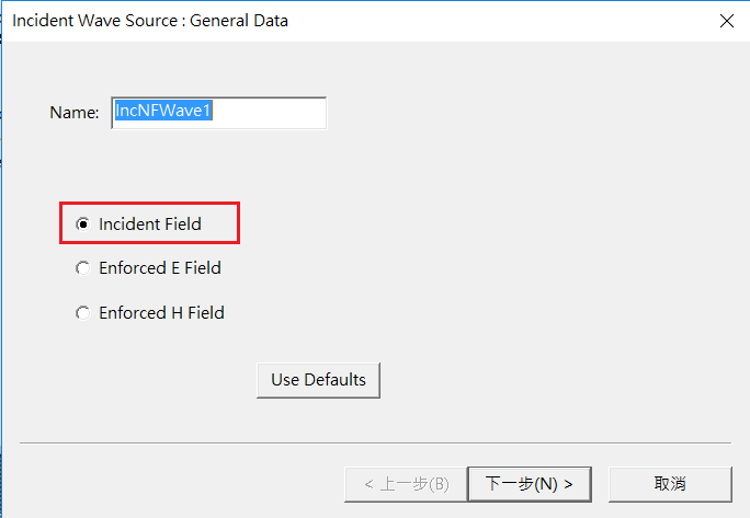
3.3 Set the radiation boundary of the box as [Incident Field] or [Enforced E\H Field]
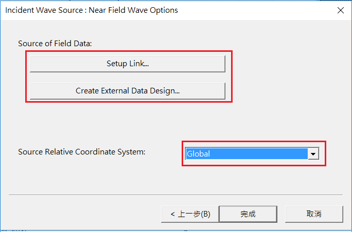
[Setup Link]是直接連結SIwave的檔案與其解完的資料內容
[Create External Data Design]是連結SIwave在1.5.1產生的.and/.nfd檔案 (建議作法)
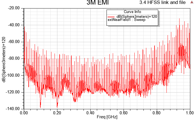
3.4 HFSS emission test result
Follow 1.4.5, C1 active
R19.2 HFSS link .and/.nfd that SIwave export (與1.4.5相比,250~260MHz沒看到明顯突出的EMI)
-
問題與討論
4.1 如何分辨真正的3D EM solver?
Ans:並非有FEM或是能show far field就是true 3D solver。筆者是以下列兩個角度判斷
-- 能解任意3D結構,比方PCB + connector,或是同一layer層中,在不同區域可有不同材質
-- 須設air box boundary,有真正求解空間場
4.2 step 1.4.2與2.1中,ETotal是什麼?
Ans:"ETotal" means the maximum of the total rE-field. When calculating the maximum far field values, the distance r is factored out of the E-field. Therefore, the units for the maximum field data values are given in volts. For SIwave, MaxETaoal is defined at 1 meter away by default.
4.3 為何SIwave跑出的遠場結果與HFSS不同?
Ans:
4.3.1 於1.4.2在R17.2 SIwave跑出的ETotal@1G最大約2.45E-10,而 於2.1 HFSS跑出的ETotal@1G最大約3.15E-5(mV)。
過去,筆者一直不知道怎麼解釋這數值的"巨大"差異(也問不到答案),還好在R17軟體UI上終於發現了原因是兩者的單位定義不同。
SIwave的場型是以mag(eTotal)表示,而HFSS是rETotal表示 ;前者單位在R17.x沒顯示(應該是V/m, at 1 meter),而後者單位在R17.x是mV在R19.x是nV/pV。(與距離無關, 距離項被乘掉了)
4.3.2 HFSS(step2.2)與SIwave(step1.4.5)解的遠場EMI level大致相同(-80~-40dB),但頻點密度不同?
本例HFSS求解出的EMI頻點比較少的主因是,HFSS求解遠場所花的時間與記憶體遠多於SIwave,所以是0~1G取100~200點掃頻的結果,而step1.4.5是0~1G取1000點掃頻的結果,所以看的頻點密度比較高。
SIwave採用HFSS與HFSS-IE的混合技術解遠場,前者以導體"實際"表面電流密度做面積分求解遠場,後者以空間中封閉面上的"等效"表面電流密度求解 ;也就是SIwave會自動幫你在空間中定義一個面,然後用採用跟HFSS相同的技術解遠場。SIwave HELP:To analyze the radiated fields associated with a design, a radiation surface is defined over which the fields will be calculated. The values of the fields over this surface are used to compute the fields in the space surrounding the device.
SIwave使用走線、貫孔、打線的電流與電源/地平面構成的腔體邊緣場當 輻射場源,這些場源乘以一個適當的格林函數(Green function),再做積分得到場值。又解近場所使用的格林函數與解遠場的不同,前者比較複雜。
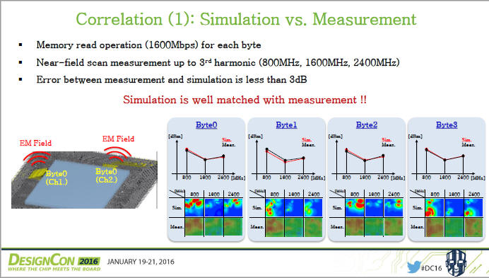
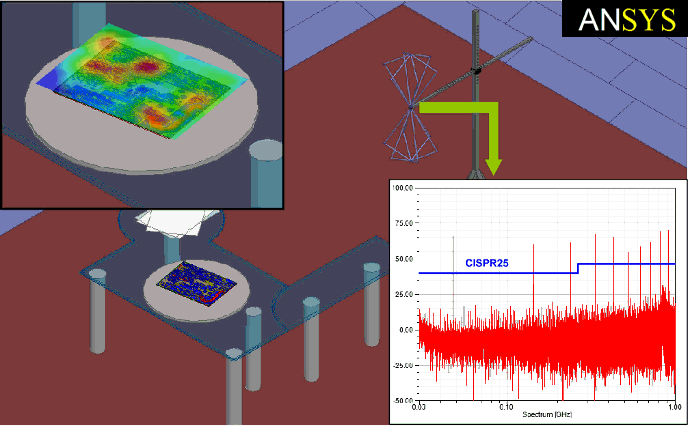
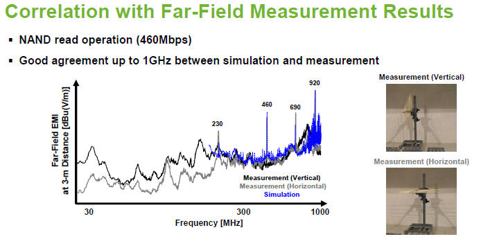
很多實際產品例子上,SIwave解的遠場結果 與HFSS是對得起來的,估計本文的例子為參考平面完整的differential pair,也沒考慮IC P/G電流帶出的影響,所以整個遠場輻射量值實在太小不好比較。有興趣的讀者也可以參考2016年Samsung於DesignCon所發表的一篇用SIwave做的800M\1600M\2400MHz EMI分析,量測與模擬correlation誤差3dB以內。[4]
4.4 為何step1.4.3中,plot遠場強度必須/3+120 ?
Ans:對於SIwave的MaxETotal [/3]代表 從1M遠處改成3M遠處所量到的遠場EMI強度,[+120]代表dBV轉dBuV的單位轉換
4.5 本文的範例附檔名.adsnz,這種檔案如何開啟?
Ans:從2013年起,ANSYS EBU產品R14.5的版本,內建整個project打包(壓縮)功能,Designer打包後的附檔名是.adsnz,要打開此類檔案只要[File] \ [Restore Archive]
從2016年起,ANSYS EBU產品R17的版本,不管是HFSS\Q3D\Designer打包的檔案,其附檔名都是.aedtz,左鍵雙擊兩下就會自動解壓開啟
4.6 Regular far field與Emission test report的差異在哪裡?
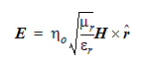
Ans:Far field是依下列公式計算,且必須先定義Radiation far field setup "Infinite Sphere"
HFSS Emission test report則是仿EMC regulation規範計算|Emax|,軟體中不須先定義Radiation far field setup極座標就可得到值
SIwave的far field report (MaxETotal)與HFSS的Emission Test Report雖然都是算|Max E|,但前者與極座標角度(Phi,Thera)相關,後者則是仿實際的EMI測試標準取最大值。故HFSS取[cylinder]是有意義的,但SIwave則不需要。所以在 新版(R17) SIwave的UI,plot far field不再出現需要指定[cylinder]的字樣。
4.7 [Max Harmonics]與[Max. Frequency]之間是甚麼關係?
Ans:查閱help了解[Window Type]與時域數值轉成FFT(頻域)有關,而更進一步的說,這是不同cut-off特性的時域轉頻域取樣技術。
在SIwave v5.0以前的版本,官方建議選[Hamming],但SIwave v6.0以後的版本,則這整個視窗都無法設定。但如果是用HFSS做dynamic link,則這整個視窗是可以設定的。
這裡的[Stop Time]來自step1.3.3的Transient Analysis的[Stop] time,又step1.4.3的頻譜解析度:[Resolution Bandwidth]=1/([Stop Time]-[Start Time]),且[Max. Spectrum Frequency]=[Max. Harmonic]*[Resolution Bandwidth]
4.8 如何取得從Designer push excitation後的excited source file?
Ans:對於SIwave,執行過push excitation後,可以從1.4.1圖中"Use sources defined in external file"的路徑下,找到SIxxx_Transient_sources.tmp檔案,其指向所有ports個別定義的.tmp file。對於HFSS,執行過push excitation後,雖然可以從Edit Source (as step 2.2)看到新定義的excited source,但真正的source data是放在[HFSS] \ [Design Dataset]內
4.9 為何讀者step1.4.2自行跑出的場型, 可能與本文所示不同?
Ans:原檔案在VCC-GND有一顆電容C1(50uF), 先把這顆電容de-active。
如果掃頻取樣從DC開始,場激發能量會變成0
如果取樣從1M開始,得到的場型
這些結果都對,會有這些差異的主因在於3D polar plot時,需要指定要繪出哪一頻點場型,否則軟體默認畫的是 所掃描的最低頻點的場型
4.10 分析遠場EMI的問題頻點,對應要看近場E還是H的熱點?
Ans:相信大部分EMC工程師都想過這問題,也基於經驗知道這答案是"不一定",但不知其所以然。
近場E場源自於電壓變化,近場H場源自電流變化。
當遠場的EMI頻點是P/G plane上的共模電流透過纜線帶出來的,該遠場頻點的基頻常會透過近場H場反應在某耗電的主IC同樣頻率的熱點。
當遠場的EMI頻點是high-speed signal (clk)帶出來的,該遠場頻點常會透過近場E場反應在該高速訊號走線區域。 Refer to here as well.
以上是個基本區分,但有時候界線是模糊的:比方說有些高速訊號振幅很低且是電流源驅動(USB20\30)。
4.11 為何step3.3中,投射incident wave的物體要設成"PEC" material?
Ans:R15 HELP內有說明,internal radiation boundary必須設成"PCE"否則不會work。
[Incident Field]是把Incident wave pattern入射於surface,其特性是absorbing boundary condition (ABC), 外面不可以再包一個ABC。如果要把[Incident Field]指定到到一個internal radiation boundary,則把被投射體整個設成"PEC" material即可。
[Enforced Field]=[Enforce H Field]則是讓Incident wave正切於surface輻射,boundary內是不考慮的,此時外面必須再包一個radiation boundary。
4.12 使用SIwave+HFSS data link (incident wave)時,如何處理PCB與機殼接地的系統级EMI模擬?
Ans:這是個非常實務,非常好的問題。
一般SIwave+HFSS data link的做法是模擬各做各的,也就是SIwave模擬PCB近場時,是沒有考慮外面機殼包覆與連接的,也就是此時SIwave沒看到機殼,當然也不會考慮與最近機殼金屬面間的藕合關係,這樣的手法往往不符合實際系統電性條件。修正的做法是:在SIwave內PCB的下方新增一個大片金屬接地平面,並透過via與PCB的GND plane連接,也就是在SIwave內用grounding via來實現接地螺絲的效應。這樣就可以在PCB四個角落的螺絲接地端,看出是否有鎖螺絲時的近場與共振模態差異。
如果一台伺服器的電源輸入由理想的三孔插座(機殼有被良好的系統接地),換成兩孔插座(機殼沒有被良好的系統接地),此時機殼內的高速電路板鎖上螺絲接機殼後,整機的EMI反而變差,這現象要怎麼模擬? 這代表高速電路板上的高頻雜訊成份,透過地迴路竄流到外部機殼,又因機殼沒有良好接地,導致機殼變成輻射天線路徑。所以此時PCB與機殼間存在高頻成份的電流流動,這樣的電性模型就無法用SIwave+HFSS data link手法做,要全部用HFSS配合Designer push excitation做。
以下的應用,就適合以SIwave+HFSS data link手法模擬
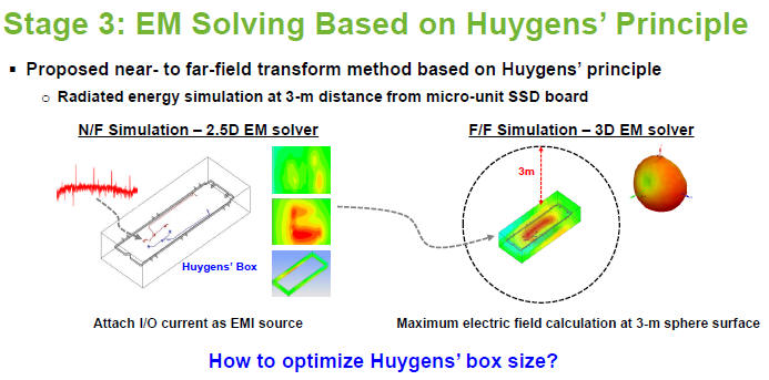
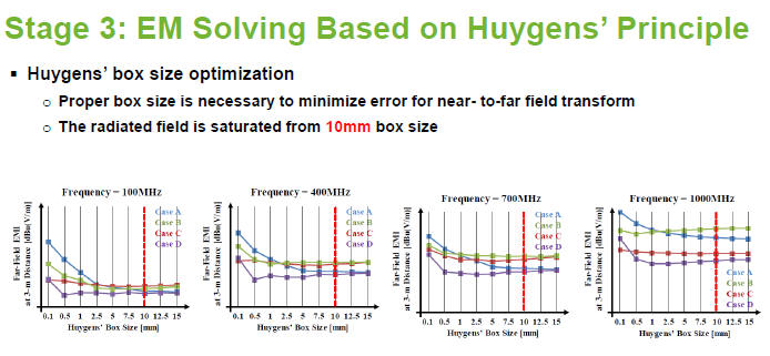
4.13 使用SIwave+HFSS data link做EMI模擬時,SIwave內near-field box size取的大小對far-filed結果有沒有影響?
Ans:有影響
在step1.5.2中我們有提到近場距離不能小於3mm,但是大於3mm是否就都沒問題呢?
2017年韓國三星用SIwave+HFSS又做了一篇含模擬與量測的比對結果,除了模擬與量測比對很準外,還建議near-field的box size取10mm。[5]
-
Reference
[1] Near field to far field transformation:http://www.ualr.edu/wirelesslab/fdtd/fdtd5.pdf
[2] Near field to far field transformation:http://www.jpier.org/PIER/pier73/05.07031903.Costanzo.D.pdf
[3] Near field to far field transformation:http://www.eecs.wsu.edu/~schneidj/ufdtd/chap14.pdf
[4] Jin-Sung Youn (Samsung Electronics), "Chip and Package-Level Wideband EMI Analysis for Mobile DRAM Devices", DesignCon 2016.
[5] Seong-Jin Mun, (Samsung Electronics Inc.), "Far-Field EMI Analysis Methodology and Verification on SSD Boards", DesignCon 2017.