線上影音
Home > ANSYS SIwave教學> Package Plane Impedance
本文始於2009年以SIwave 4操作,2014年以SIwave2014 with Alink重新撰寫。
問題與討論
10.1 What is the behavior of "Pin Group"?
10.2 How does SIwave solve solderball effect?
10.3 Why do the bond wires seem to not touch traces (finger pad)?
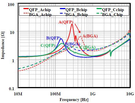
10.4 How is the Z profile difference between different package type?
10.5 Why does it get totally different Z profile with 0.1uF and 1nF decap.?
![]()
-
Import ANF (Ansoft Neutral File) files

-
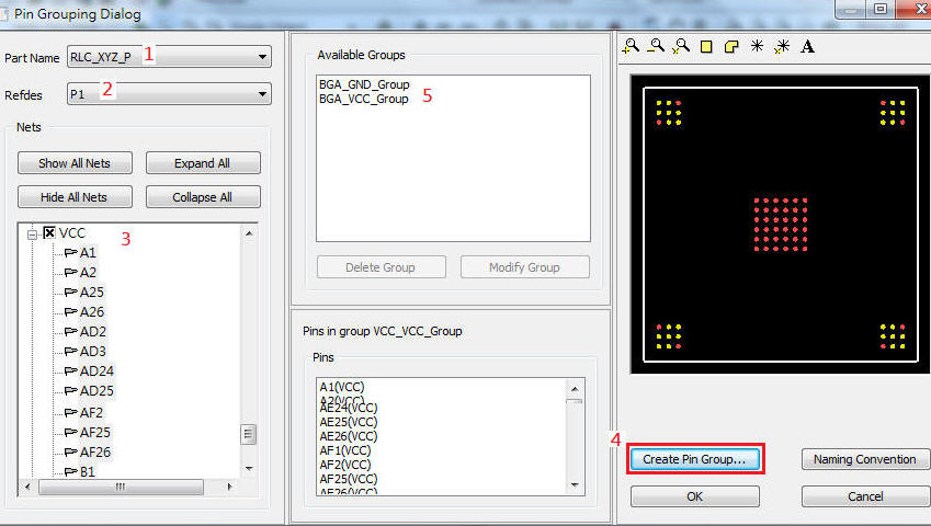
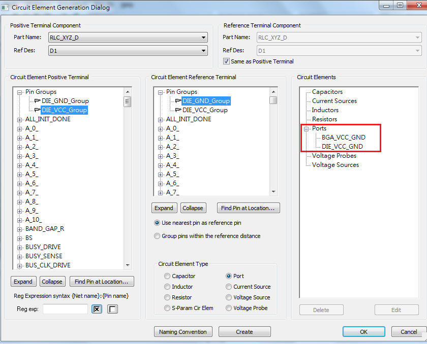
Group VCC and GND pins on both the die and ball sides
- 正確的選擇所要group的Part Nme="RLC_XYZ_P"與reference designator,左邊的Nets list會自動更新
- 核選要group的net,此時就可以在右邊的顯示畫面看到該net的位置
- 進一步將此net展開,下拉選定所有的pin name,此時會看到所有GND pins都high-light,此時"Create Pin Group"按鈕才可以作用
- 按下"Create Pin Group",會跳出一個預設名稱的對話確定框,按確定
- 在"Available Groups"框內就會出現該Net group name
- 同樣方法,Net VCC也建一個Group (rename to BGA_VCC_Group)
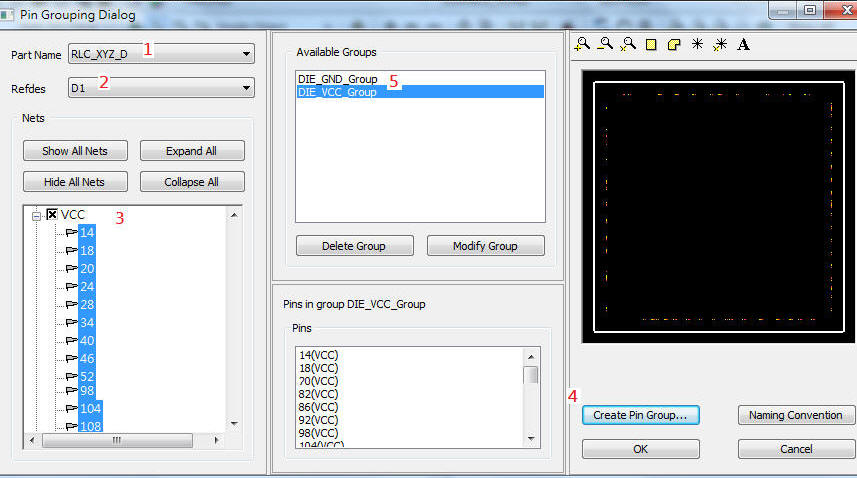
- 正確的選擇所要group的Part Name="RLC_XYZ_D"與reference designator,左邊的Nets list會自動更新
- 其餘步驟與上述建立BGA VCC\GND net group的方法相同
-
問題與討論
File \ Import \ ANF
.anf與.cmp of BGA該如何得到,是封裝廠提供嗎?
封裝廠使用Cadence Allegro Silicon Package Board (SPB)做BGA的substrate設計,產生.mcm或.sip檔, 只要安裝ECAD就可以轉出.anf。這檔案轉換的程序,需要有ALink(舊稱AnsoftLinks)與ECAD translator,前者在import .anf需license,後者轉出.anf不須license。
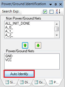
Power/Ground Identification
Edit \ Validation Check
Simulation \ SIwave \ Options
File \ Save as (.siw)
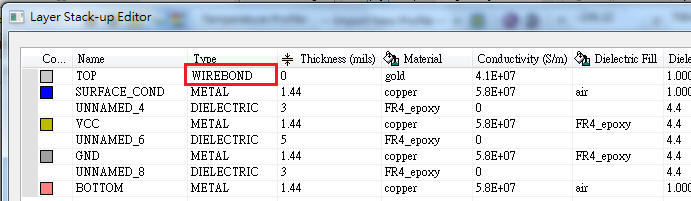
Edit \ Layer Stack
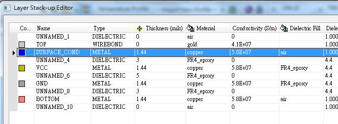
選定空氣介質層,按Delete刪除。比較特別的是有TOP layer的"WIREBOND" type
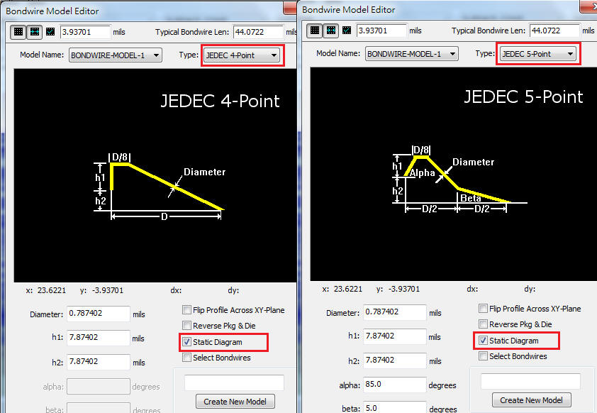
Edit \ Bondwire Model ![]()
SIWave提供 數種Boundwire model:for example,JEDEC 4-Point、JEDEC 5-Point,只要勾選"Static Diagram"就可以了解h1、h2參數的意義
Edit \ Solderball Model
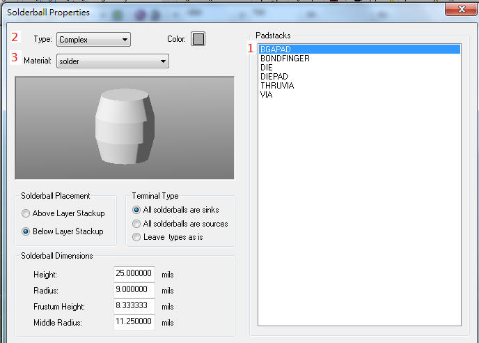
Solder balls這一層的高度,就是錫球高度25mils。
Tools \ Pin Group Manager
To Group all GND and VCC balls individually (選定BGA端的Net點, Ball location)
To Group all GND and VCC bondwires (選定Die端的點, Die Pad location)
Circuit Elements \ Generate on components
Create Ports on BGA side
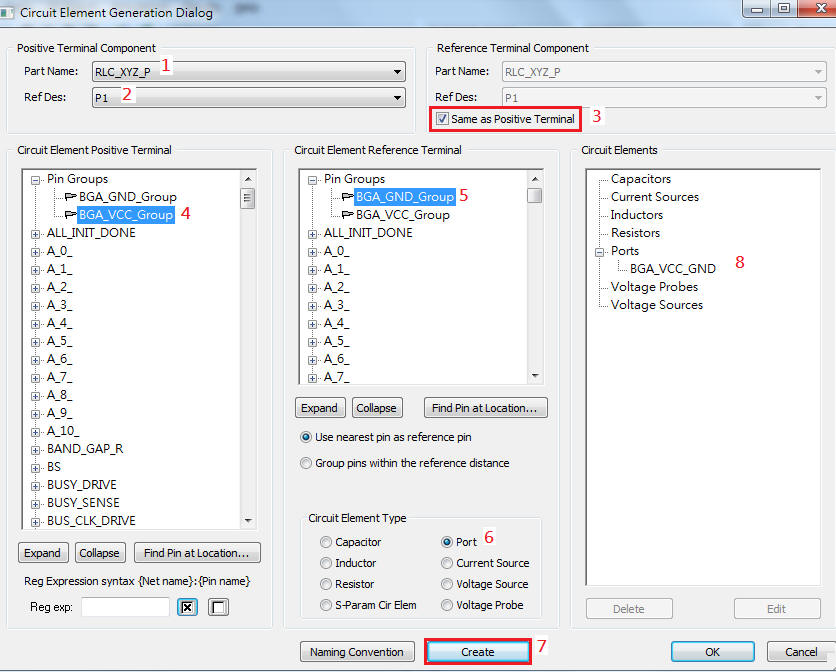
Create Ports on DIE side
Simulation \ Compute S-, Y-, Z-parameters
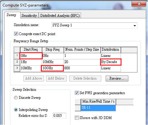
![]() "Start
Freq"選擇1Hz或0Hz,對後面跑Z-parameter
plot模擬結果的低頻部份,以上圖的建議設定,加強低頻取樣較好
"Start
Freq"選擇1Hz或0Hz,對後面跑Z-parameter
plot模擬結果的低頻部份,以上圖的建議設定,加強低頻取樣較好
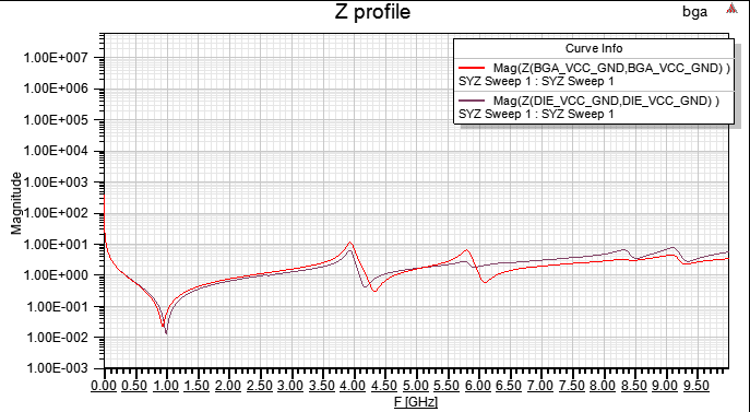
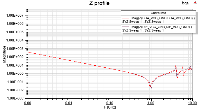
執行模擬後,會彈出Reporter視窗。
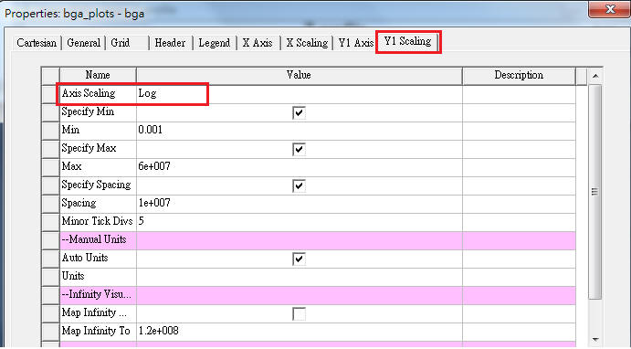
調整Y軸刻度顯示單位如下(改成Log顯示)
調整後的顯示如下,可以看出power與ground plane之間是高阻抗的(絕緣),所以隨著頻率的降低,阻抗飆升。
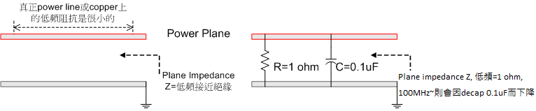
實務上低頻的Z of PWR-GND會被板子上的大電容壓下(as 100uF),所以一般看Z profile主要在觀察中高頻的部分(above 10MHz~100MHz),若模擬時在power-ground plane之間跨一個1歐姆小電阻,可便於觀察高頻的Z profile。
可以看出整個bonding + substrate design的plane impedance在0~1.1GHz阻抗<1歐姆 ,1.2GHz以上會劇增到 最大約8歐姆。(肌膚效應,skin effect)
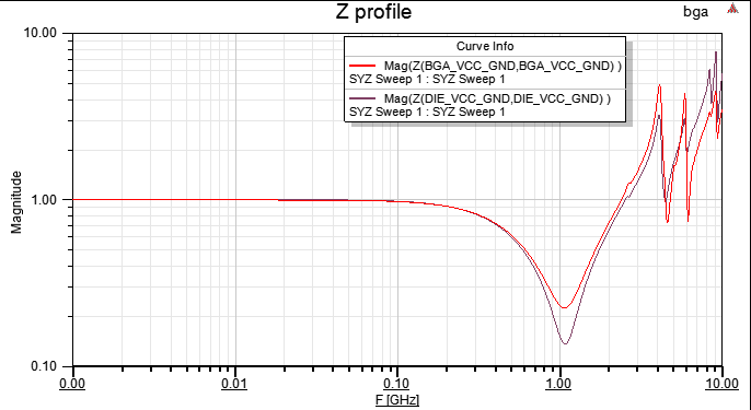
若在BGA內四個角落的substrate夾層,加四顆0.1uF "buried de-coupling capacitor",模擬結果如下所示;在5MHz~110MHz的阻抗都壓到0.1歐姆以下
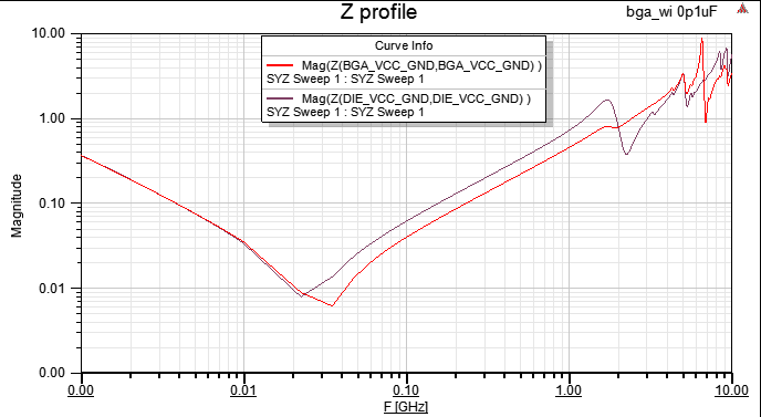
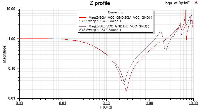
若在BGA內四個角落的substrate夾層,加四顆1nF "buried de-coupling capacitor",模擬結果如下所示:阻抗最低點往高頻移動
10.1 What is the behavior of "Pin Group"? ![]()
Ans : The grouped pins will be treated as if they were electrically connected during the analysis. (PEC connect)
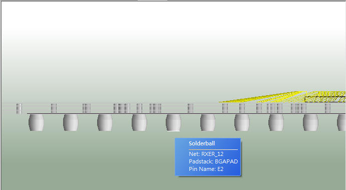
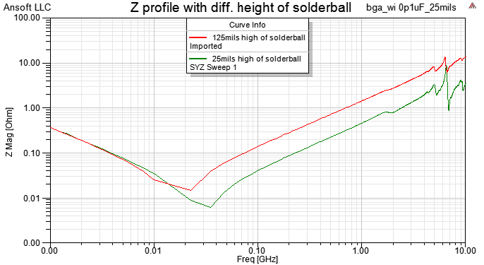
10.2 How does SIwave solve solderball effect? ![]()
Ans : SIwave is able to get different SYZ result with different height of solderball, but there is no mesh on it.
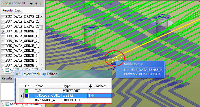
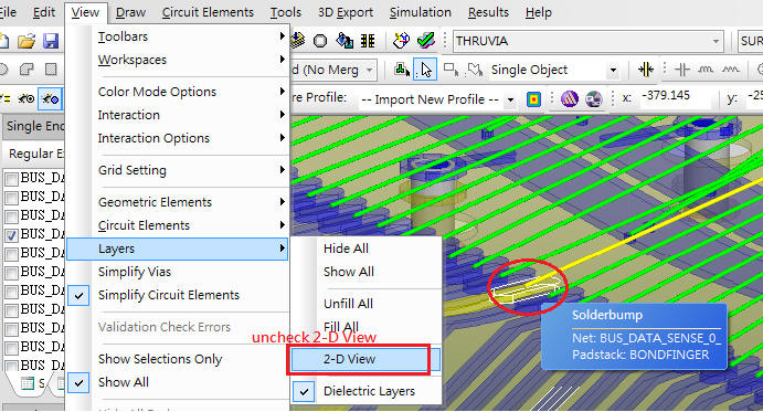
10.3 Why do the bond wires seem to not touch traces (finger pad)? ![]()
Ans : The metal layer is displayed as sheet for rendering efficiency by default in SIwave, and you can disable the [2-D View] option.
10.4 How is the Z profile difference between different package type? ![]()
Ans : Please refer to [1]
10.5 Why does it get totally different Z profile with 0.1uF and 1nF decap.? ![]()
Ans : because of different SRF (self-resonant frequency)
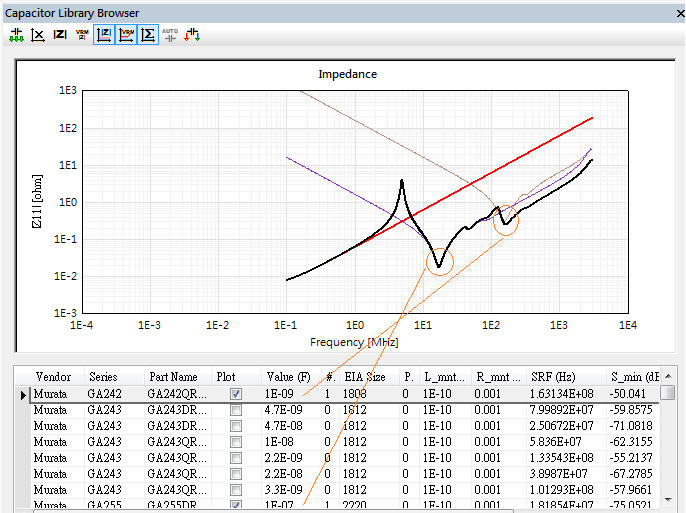
上圖電容的自振頻率(SRF)與Z profile對不起來的原因是,Z profile有考慮了L_mnt, R_mnt
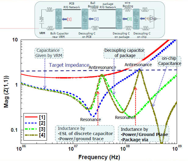
[1] M. Terasaki, S. Kiyosige, "Power Integrity Behavior for Various Packaging Environments", 2013.
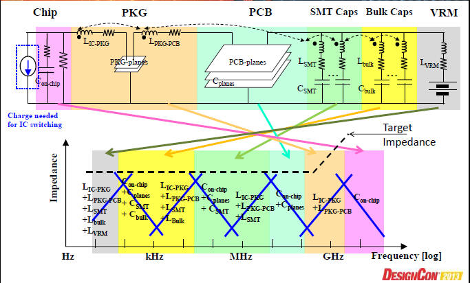
[2] K. Shringarpure, S. Pan, "Innovative PDN Design Guidelines for Practical High Layer-Count PCBs", DesignCon2013. (推薦)
[3] C.H. Lin, C.C. Wang, "System Power Integrity Impact by Package Power/Ground Balls Assignment and Decoupling Capacitors", 2012.
[4] Tzong-Lin Wu, "Power Integrity and EMC Design for High High-speed Circuits Packages", 2008. (推薦)