線上影音
Home > ANSYS SIwave教學> PBGA and PCB co-simulation
本文介紹PBGA與PCB的整合模擬,並以DDRII與USB differential pair為例說明。除了敘述如何設定PBGA內substrate的堆疊與bonding wire外,還以實例示範幾招debug技巧,找出模擬波形差的原因。從模擬結果發現,For this case, PCB level對SI貢獻較多Jitter (via ISI, not length matching),而PBGA level則是貢獻較多overshoot\undershoot。
-
環境與參數設定
-
5.1 模擬結果
5.2 Debug過程
5.3 單獨看PBGA效應
5.4 單獨看PCB效應
-
7.1 Export S-parameter (.snp)
-
問題討論
-
Reference
1.1 .mcm轉成siw
1.2 堆疊與參數設定
1.3 Bonding Type
![]()
-
環境與參數設定
封裝廠使用Cadence Allegro Silicon Package Board (SPB)或Advanced Package Design (APD)做BGA的substrate設計,產生.mcm檔,可以轉成.siw。
1.2 堆疊與參數設定
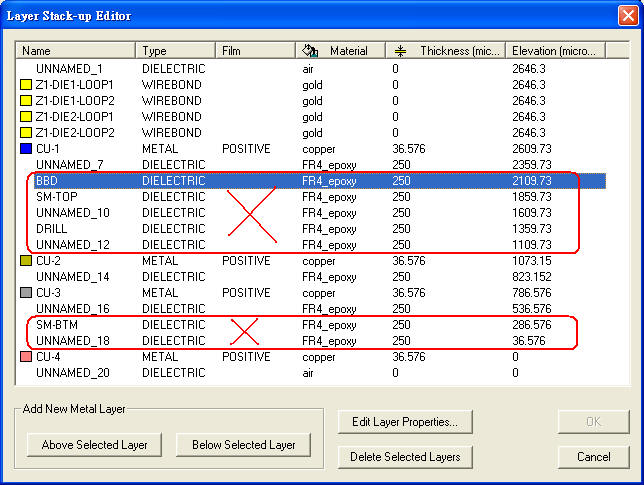
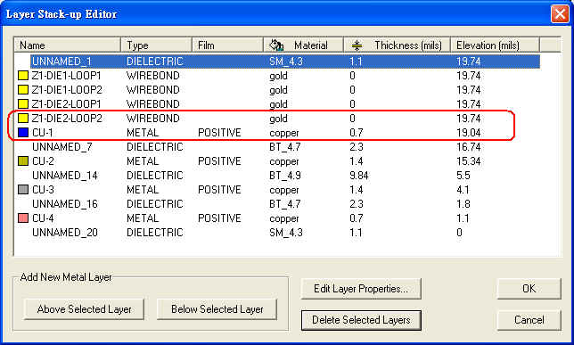
1.2.1 從.mcm轉出的.siw,打開堆疊設定選項Edit \ Layer Stack,一開始會看到如下圖所示,有一些多餘的layer需要刪除
1.2.2 堆疊高度與介質的介電係數也要設定 (相關參數可請封裝廠提供),完成後如下圖所示
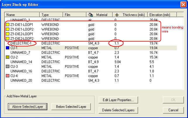
以上圖設定來說,在top layer上方加一層solder mask layer,原意是想模擬top layer上的絕緣綠漆對特性阻抗的效應,但這樣的設定,在SIwave v3.5卻會導致bonding wire與finger pad電氣不連接,bonding wire浮在trace上,如下圖所示
1.3 Bonding Type
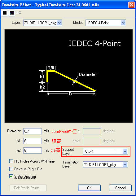
1.3.1 Edit \ Bondwire Model:設定Bonding type、Bonding wire width、Die thick
SIwave v4.0以後的版本,多了[Support Layer]、[Termination Layer]讓user可以指定打線的起點與端點的層面(上圖所示)。所以SIwave v4.0以後的版本,可以藉由正確的設定[Support Layer]、[Termination Layer]來讓substrate上存在solder mask與compound\moldinglayer。
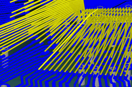
如果die同一側有兩排pad,那外側排pad的弧高較低,內側排pad的弧高較高。整個完成後,我們可以檢查一下,bonding wire是否與substrate top layer上的finger pad有連接,如果發現bonding wire浮在半空中,那可以檢查Edit \ Layer Stack設定,是否在top layer與bonding wire之間有其他介質層未清除。
若沒正確設定晶片高度(厚度),Validation Check時,可能會誤判成Die pad與Die正下方的導線短路。
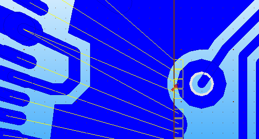
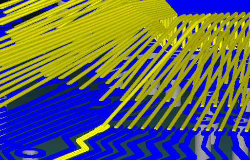
1.3.2 下圖我們把原本在top layer上的Solder Mask layer移到最上層,讓top layer與bonding wire之間沒有其他layer,且bonding wire Z1, Z2, Z3, Z4的高度設0,所以同樣能模擬到SM layer的影響。
下圖可以看出,bonding wire已經埋到top layer的finger pad裡,整個net的電氣特性有連在一起了
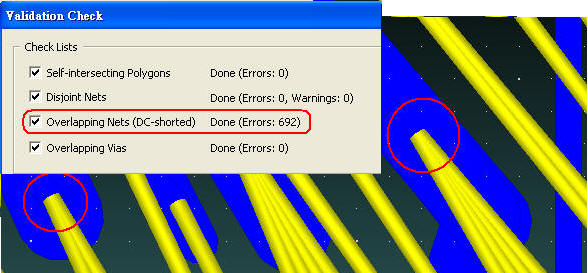
Edit \ Validation Check
BGA設計的Validation Check,很容易碰到"Overlapping Nets" Errors,主要原因是SIwave v3.5會把double bonding與triple bonding...等,視為短路,這種Error可以忽略不管,並不影響後面的模擬。
請參閱本站Merge PCB and BGA design一文
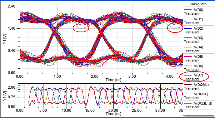
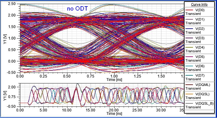
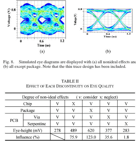
A 4-layer PCB follows neither length-matching nor 3W design rule and PBGA-300pin with [plating process] 4-layer substrate。觀察一組point-to-point的DDRII data group走線(D0-7, DQS, /DQS, DQM),half-drive mode without ODT,並用PRBS (Pseudo-Random Bit Source)作為眼圖模擬pattern。
A 4-layer PCB follows both length-matching and 3W design rule and PBGA-500pin with [non-plating process] 4-layer substrate。觀察一組point-to-point的DDRII data group走線(D0-7, DQS, /DQS, DQM),half-drive mode without ODT,並用PRBS (Pseudo-Random Bit Source)作為眼圖模擬pattern。
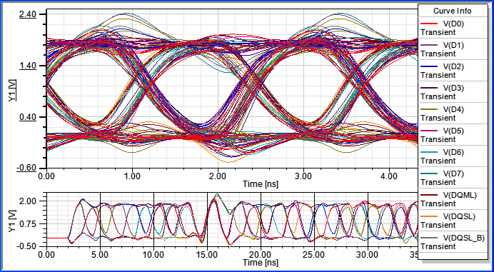
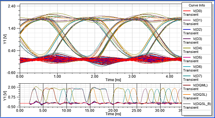
5.1 模擬結果
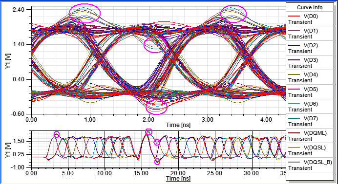
不論是sec.4或sec.5.1的模擬結果,發現在訊號被同步拉高或拉低時,D1,D4,D7,DQSL會出現特別差的overshoot\undershoot,筆者懷疑是crosstalk造成 。不用改layout,只要 在SIwave內改一下模擬設定(不考慮線與線之間的coupling),再跑一次模擬就知道是不是這原因。
5.2 Debug過程
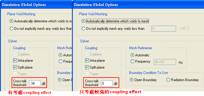
5.2.1 在Simulation \ Options做如下設定,提高考慮coupling效應的門檻
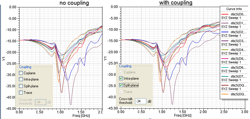
模擬結果還是與sec 5.1相同
5.2.2 在Simulation \ Options做如下設定,完全不考慮線間的coupling effect
模擬結果還是與sec 5.1相同。
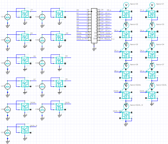
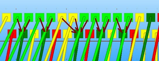
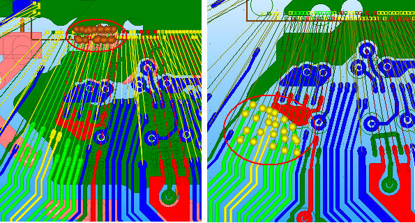
筆者此例所有ports是直接下在DIE PAD上,且每個訊號的negative terminal下在就近的ground pad(下圖深綠色pad),這樣的作法,不管有沒有考慮[coupling effect],只要有考慮bonding wire,overshoot\undershoot就比較大。
5.2.3 在Designer\Nexxim內設定,把D1,D4,D7,DQSL以外的port,input pattern都設always 0
同樣的訊號,模擬結果overshoot\undershoot明顯比sec 5.1好很多
5.2.4 在SIwave內設定,把D1,D4,D7,DQSL以外的port都de-activate
模擬結果overshoot\undershoot明顯比sec 5.1好很多
5.2.5 在SIwave內設定,把bonding wire線徑從0.7mils加粗到1.2mils
模擬結果還是與sec 5.1相同
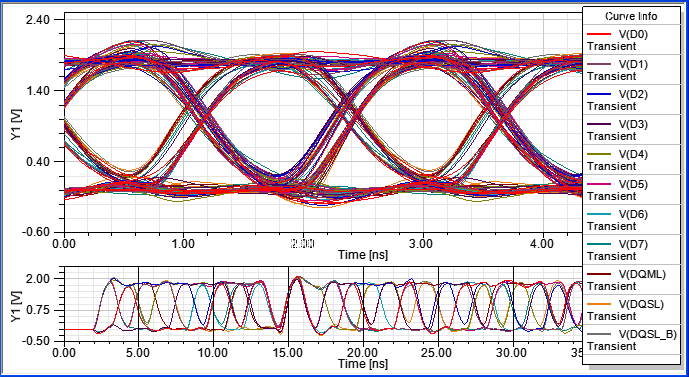
5.2.6 在SIwave內設定,把die pad端的port移到substrate上,並且negative terminal of port下在正下方內層的GND plane,以排除PI issue (排除多條線的return path透過同一段bonding wire走,或bonding wire產生的3D return loop area,或bonding wire之間的coupling效應)
同樣的訊號,模擬結果overshoot\undershoot明顯比sec 5.1好很多 ,這非常接近sec.5.4的模擬結果。所以整個PBGA對SI惡化所貢獻的issue,都集中在從substrate finger to die pad這一段上,可能是return path loop、bond-wire type,或bonding wire之間的coupling effect。
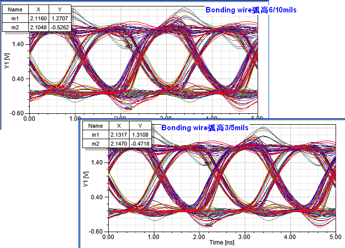
5.2.7 在SIwave內設定,把bonding wire弧高從6\10mils,改成3\5mils
模擬結果比sec 5.1稍微好一點點
5.3 單獨看PBGA效應
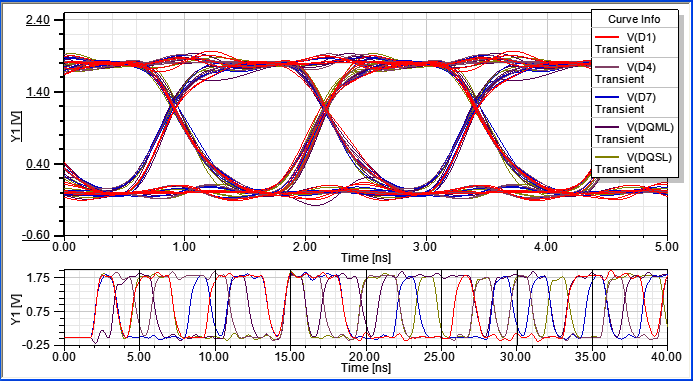
單獨模擬BGA時,D7與DQSL的overshoot\undershoot就比較差了; 但若只對D1,D4,D7,DQM,DQSL下port,則波形如下,好的很
5.4 單獨看PCB效應
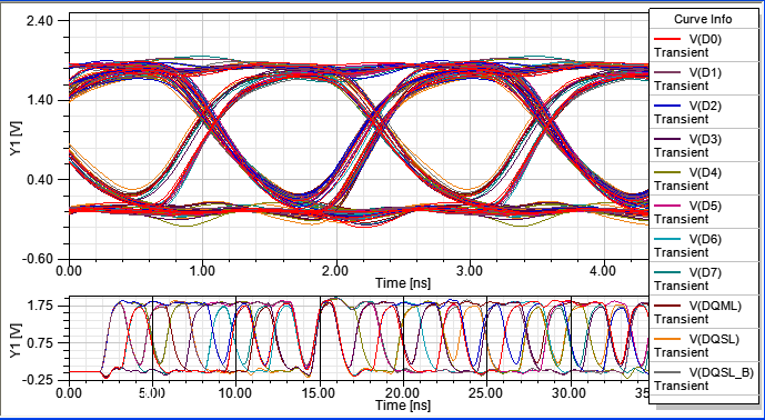
除了D6比較好以外,其餘每個訊號眼圖疊起來,"自己的"時間差(jitter)就蠻大的。 這是因為模擬的source pattern是用(PRBS),考慮crosstalk-induced jitter與Data-Dependent Jitter(DDJ)效應共同影響。讀者可以比較source pattern用PRBS與CLK的眼圖差異,後者會細很多。
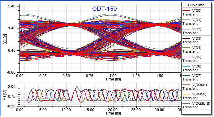
A 4-layer PCB follows just 3W design rule and PBGA-500pin with [non-plating process] 4-layer substrate。觀察一組point-to-point的DDRII data group走線(D0-7, DQS, /DQS, DQM),half-drive mode with/without ODT,並用PRBS (Pseudo-Random Bit Source)作為眼圖模擬pattern。
7.1 Export S-parameter (.snp)
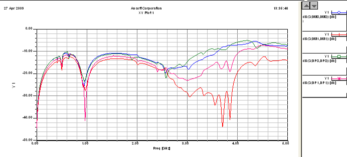
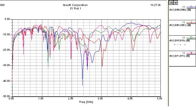
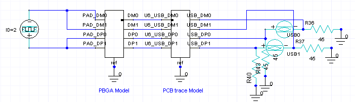
7.1.1 在USB differential pair的die pad端與PBGA ball-out端,分別下ports
7.1.2 執行Simulation \ Compute S-, Y-, Z-parameters,做S參數分析
7.1.3 Results \ S-,Y-,Z-parameters \ Export to Touchstone Files,吐出.snp file
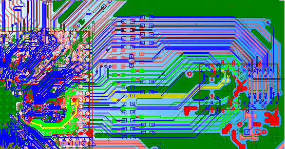
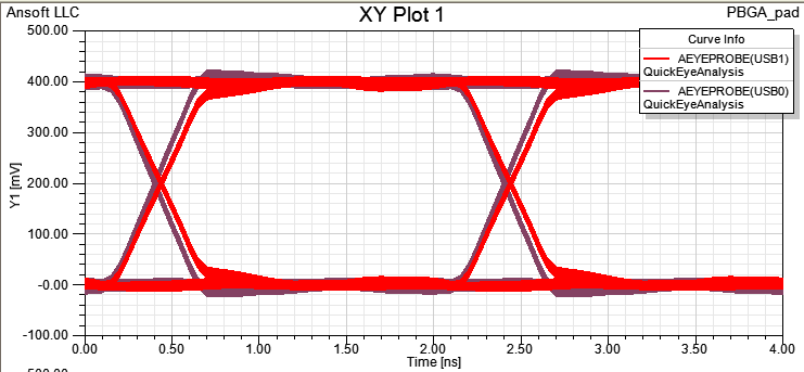
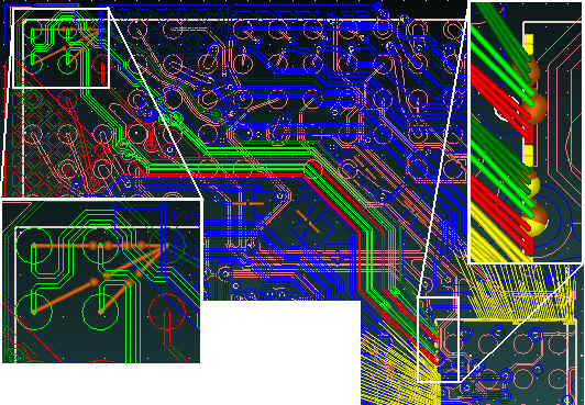
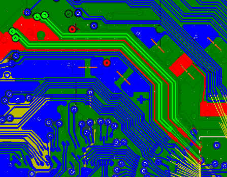
7.1.4 一開始的BGA substrate設計,因為在BGA內部有放SMD 0.1uF電容,導致USB pair往右上彎曲走線,造成走線跨地現象。下圖紅色net代表USB 3.3V power,深綠色代表USB GND,淺綠色則代表USB differential pair。
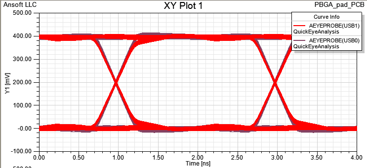
7.1.5 以Design/Nexxim模擬從die pad to BGA ball的眼圖與S11波形如下
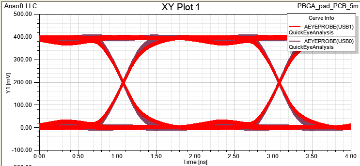
7.1.6 以Design/Nexxim模擬從die pad to BGA ball + PCB trace effect的眼圖波形如下,約多0.53ns相位延遲,相當於USB trace在PCB板子microstrip上走了(530ps/160ps)*1000mils=3312mils。(實際值3175mils,很接近了)
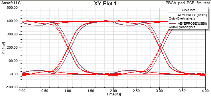
7.1.7 以Design/Nexxim模擬從die pad to BGA ball + PCB trace effect + 5M cable with CL=5pF的眼圖波形如下
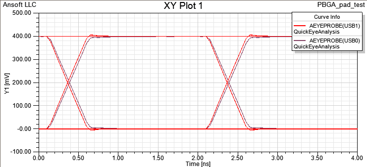
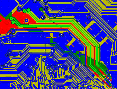
7.2.1 在SIwave試著把USB pair走線下方的ground plane補起來
7.2.2 重新跑S-parameter並重新模擬,以Design/Nexxim模擬從die pad to BGA ball的眼圖與S11波形如下
7.2.3 以Design/Nexxim模擬從die pad to BGA ball + PCB trace effect + 5M cable with CL=5pF的眼圖波形如下,USB1改善明顯
問題與討論
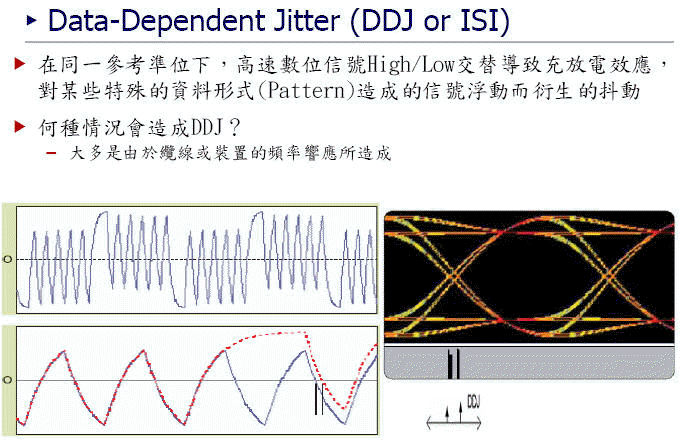
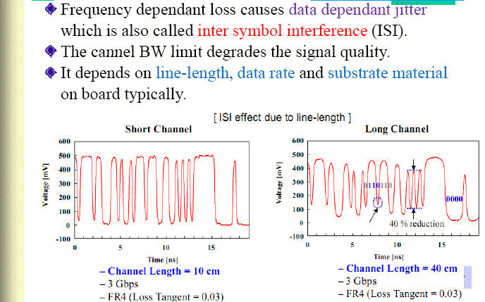
8.1 何謂DDJ、ISI,其worst case?
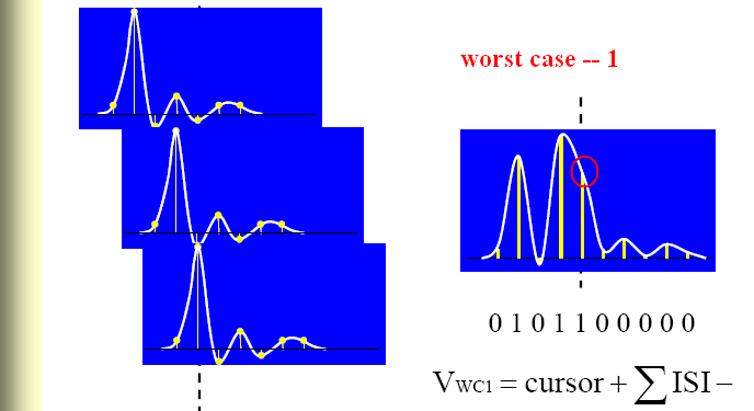
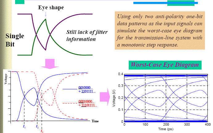
8.1.1 Data-Dependent Jitter (DDJ)、Inter symbol Interference(ISI):會依前幾個bit是否轉態,影響到傳輸線訊號 當下轉態瞬間,需要改變傳輸線C極性的難度或開始轉態時的電壓準位,即影響訊號edge傳遞速度與眼圖
盡量縮短傳輸線總線長
減少傳輸線的損失(縮小return loop, 縮短stub)
拉寬與鄰線的距離
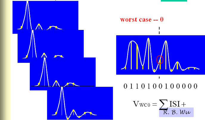
8.1.2 以下四張圖是台大吳瑞北老師的講義內容,說明ISI的worst case pattern for fast-eye analysis
8.1.3 Crosstalk induced jitter
8.2 PCB與BGA的整合模擬,以sec. 4,5,6的作法,把兩者在SIwave內先merge起來,吐出一個.snp到Designer\Nexxim做模擬;或是用sec. 7的作法,兩部份個別產生.snp,再到Designer\Nexxim連結做模擬。這兩種作法差在有無考慮錫球的3D立體結構,模擬結果差多少?
Reference
[1] IC package and PCB co-design. 重點請看p6, p22~
[2] James F. Buckwalter, "Cancellation of crosstalk-induced jitter", IEEE Journal of Solid-State Circuits, 2006.
[3] Hao-Hsiang Chuang, Wei-Da Guo, "Signal/Power Integrity Modeling of High-Speed Memory Modules Using Chip-Package-Board Coanalysis", IEEE Trans. on Electromagn. Compat., 2010. (推薦)
[4] Tzong-Lin Wu, "Power Integrity and EMC Design for High High-speed Circuits Packages", 2008. (推薦)
[6] Randy Wolff, "Signal Loop Inductance in [Pin] and [Package Model]", DesignCon IBIS Summit 2010