Online video
Home > ANSYS Designer 教學 > ESD Gun Model and ESD Simulation
This article started in 2011 and was revised in 2013, 2019 and 2022. It introduces three methods to implement ESD Gun model using the Designer circuit level and HFSS field level and demonstrates the indirect discharge according to IEC61000-4-2 regulation. It should be the first time you see such a subject showed with some discussions in detail.
![]() In the past, transient solution type (TD solver) is a HFSS "option".
Since R19+, it has been added to HFSS by default.
In the past, transient solution type (TD solver) is a HFSS "option".
Since R19+, it has been added to HFSS by default.
-- Update the figure in 3.1 and 3.2 on 2022.11.10
-
ESD Gun Model by Designer Circuit 2019 R1
2.2 ESD Gun Model following [3][4]
-
ESD Gun Model by HFSS 2019 R1
-
System ESD Simulation
4.1 System ESD simulation know-how
4.3 System ESD simulation
4.3.1 ESD discharge to ground plane with HFSS v15
4.3.2 ESD discharge to a microstrip line with HFSS v15
4.3.3 Vertical Indirect Discharge Simulation with 2019 R1 HFSS
-
Q&A
5.1 Any relationship between IC and System ESD? (important)
5.2 How to plot S-parameter under Transient mode?
5.3 How to plot Field result for transient solve?
5.4 Can lump RLC boundary be used on a solid object?
5.5 Can HFSS simulate CDM (Charge Device Mode) ESD?
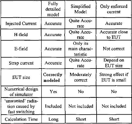
5.6 What differences are between the 3 kinds of HFSS ESD Gun?
5.7 What factors will affect the speed of HFSS Transient Solver?
5.8 To observe voltage/current of ESD, should we check E-filed or H-field?
5.9 When ESD discharge, the grounding end of ESD gun strap will shine or not?
5.10 What is the difference between Lump Port or Voltage Source for Transient solver? (important)
5.11 How to detect ESD soft failures (Class B) and find the root cause to improve?
5.12 What is the difference between Composite Excitation and Network Analysis of Transient solver?
![]()
-
EMC Regulation about System ESD

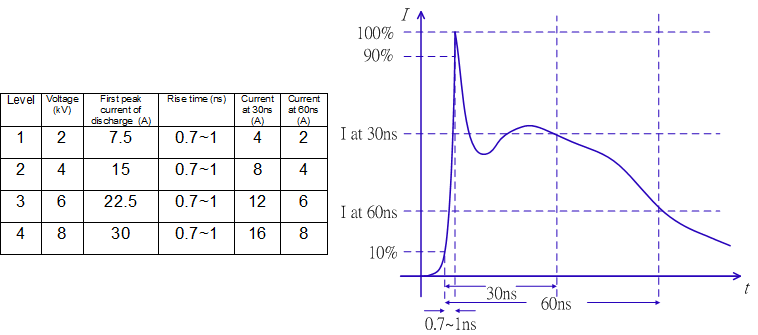
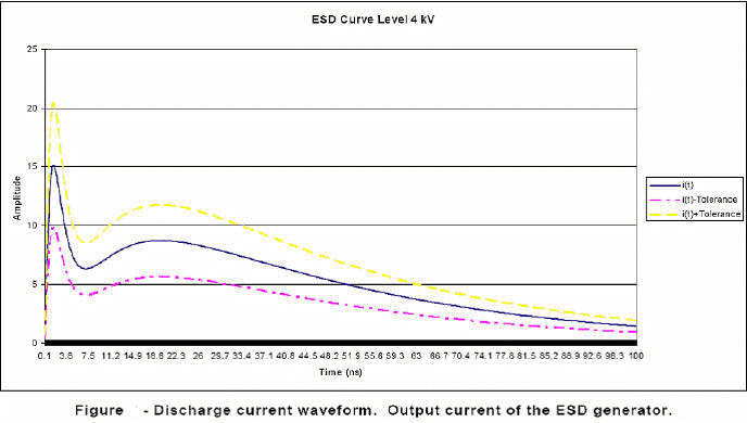
1.1 IEC-61000-4-2 or EN-61000-4-2 p.19
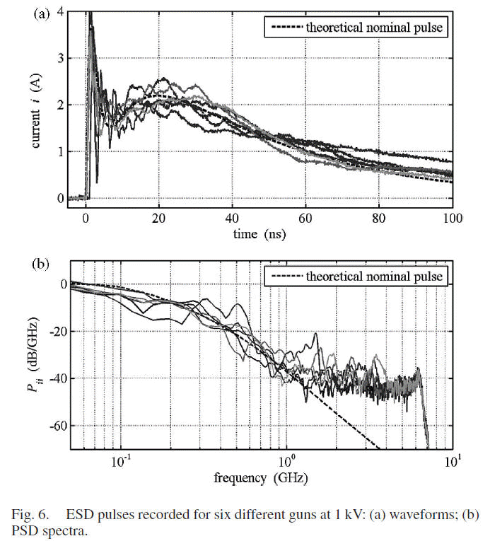
As can be seen from this diagram, EMC regulations define the output of an electrostatic gun with a current waveform. The output energy is divided into two bands; the rise time of the first band is very short (0.7~1ns), but the current peak is extremely high (3.75A/KV). It reflects the result that charges instantly release from the arm. The second band (10~60ns) is that it reflects the release result of the body's accumulated charge.
Take notice of three points : 1. 1'st Ipeak=3.75A/KV. 2. the highest level of 2'nd discharge stage appears before 30ns. 3. the current level at 60ns is half of the one at 30ns.
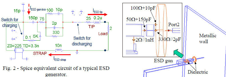
1.2 ESD Gun Model
1.2.1 Basic models provided by regulations (EN-61000-4-2 p.17)
From this diagram, it can be seen that the ESD gun/generator model, in addition to the RLC lump, also requires two sequential staggered switches to achieve charge and discharge control.
A relay implements these two "switches", and some extra RLC parasitic will be induced as well.
1.2.2 ESD gun model from foreign textbooks
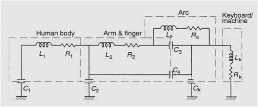
Although the above model covers the air discharge path linking to the load, the "arc" behavior with an RLC equivalent network, that is only regarded as a behavior model. It does not react to the electric field caused by an arc phenomenon in which water molecules in the air are instantaneously dissociated. Refer to 4.1, 5.18
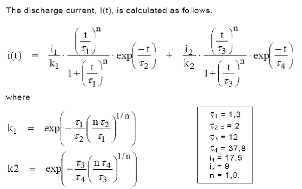
1.2.3 Regulations Define the mathematical equation of discharge current (IEC-61000-4-2 , Part 4-2)
- ESD Gun Model by Designer Circuit 2019 R1
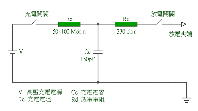
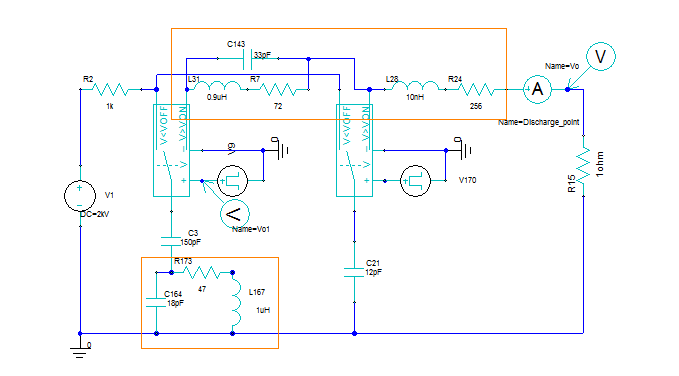
2.1 Discharge model of body (135~150pF) and arm (12~15pF) is simulated by two-stage RLC, and the output is observed by V_probe and I_probe
Both of the two switches above are turn-on at 1ns, and you can download the example to understand how it works.
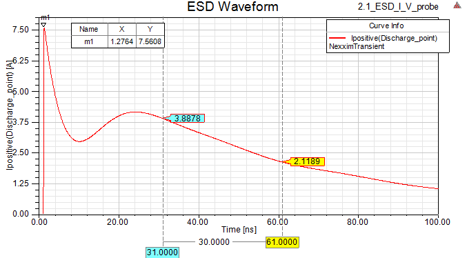
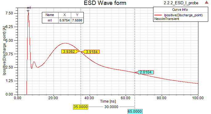
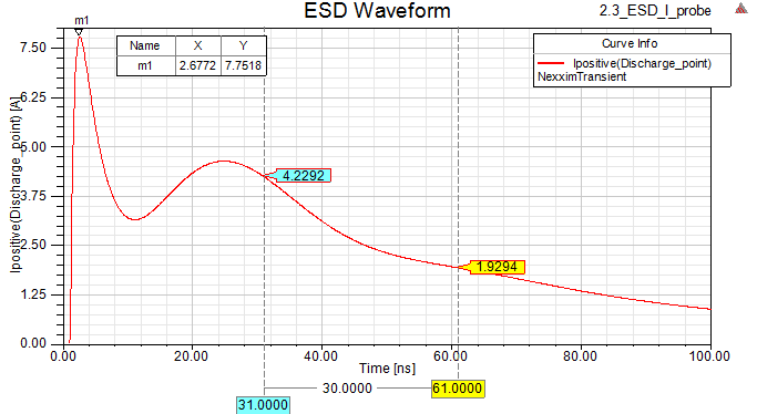
Verify if the result meets the discharge current waveform defined by the regulation:
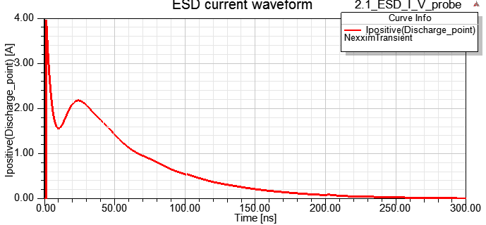
2KV : I peak = 7.5A, I = 3.9A at 30ns is ok, the first current peak appears at 1.2-1 = 0.2ns, and the second current high wave appears before 30ns.
(C21, R24) directly affects the magnitude of the first I peak, and (L31, R7) directly affects the peak value of the second segment discharge (25 ns) and the time of occurrence. The parasitic RLC of the charging capacitor C3 to the ground path affects the recessed characteristic between the first current peak and the second current peak, which is critical to the ESD Gun. [4]
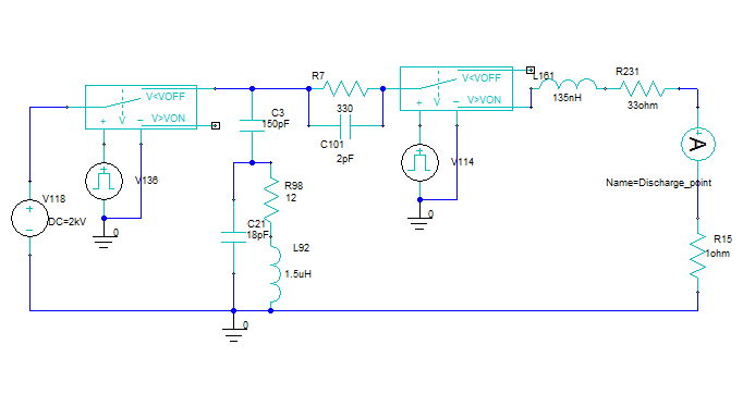
2.2 The basic ESD gun model provided by the regulations, adding parasitic RLC of ground strap[3][4]
Use I_probe to verify (with 2KV discharge)
Both of the two switches above are turn-on at 5ns, and you can download the example to understand how it works.
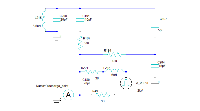
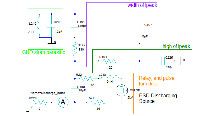
2.3 ESD Gun equivalent model by [2][6]
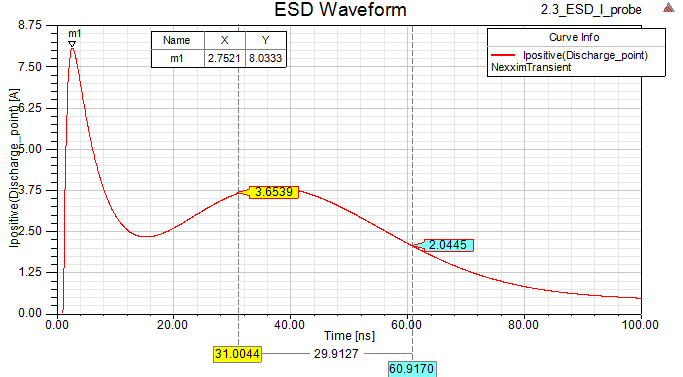
Although this model is based on IEEE Trans. papers, but the current waveform is a bit different from regulation's definition:
the highest point of 1'st current waveform stage is at 2.7-1=1.7ns (more than 0.7~1ns), and Ipeak=8A (bigger than 7.5A)
the high point of 2'nd current waveform stage is after 30ns (slower), and Ipeak=3.6A at 30+1ns (smaller than 4A)
Modify (L215,C200) from (3.5uH,20pF) to (2uH,12pF), and modify the charge caoacitor C191 from 110pF to 135pF, the current waveform much better.
As [2] mentioned, the charge capacitor of ESD Gun is 150pF, but 110pF is used for simulation, it is because to fit measurement.
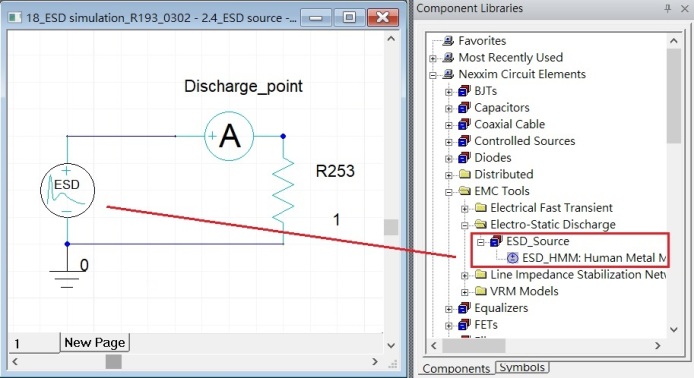
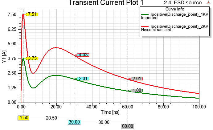
2.4 Designer built-in ESD Gun Model from R19.0
From Designer circuit R19.0, ESD/EFT source are build-in, and users can take it to simulate ESD/EFT directly and easily.
-
ESD Gun Model by HFSS 2019 R1
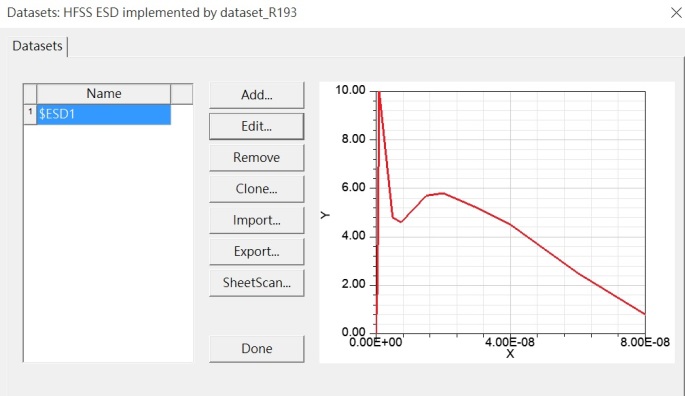
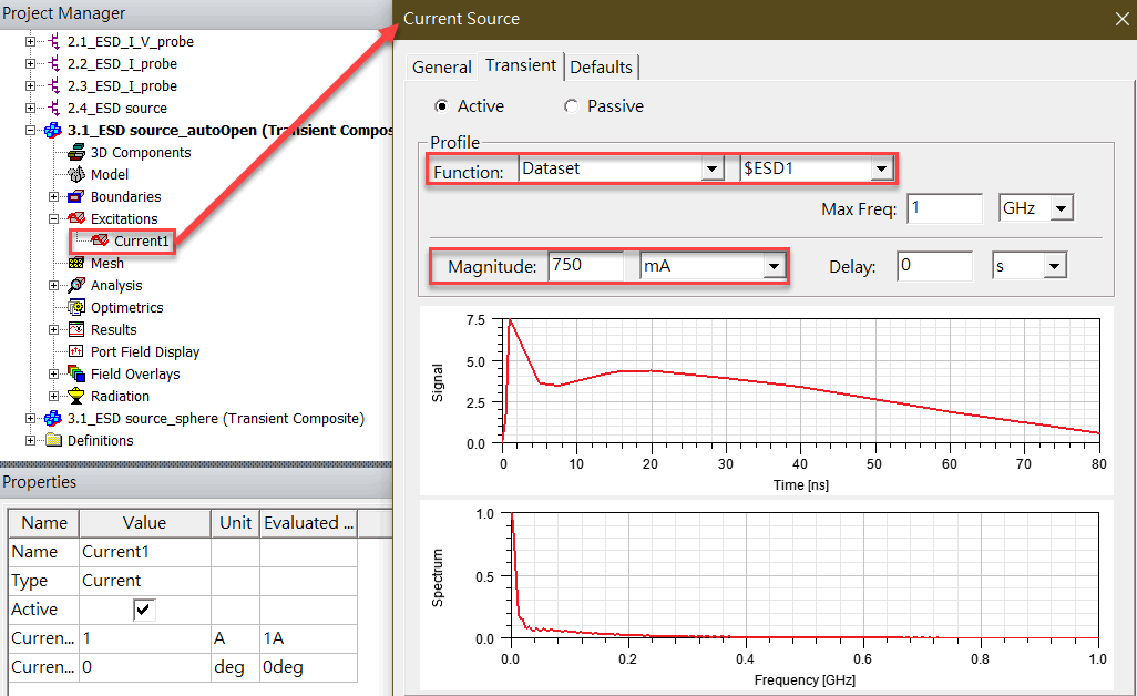
3.1 Use "Current Source" with current profile definition from "Dataset"
[Project] \ [Datasets]
Add "current source" as an excitation
Double-click terminal of "current source" to assign dataset pattern (under Composite Excitation mode of solution type)
Due to involving low frequency energy, the sphere air box is suggested ESD simulation instead of a cube one (or Auto-Open option), even sometimes the auto-open seems to be ok as well.
| Use auto-open radiation outer boundary | Use radiation outer boundary with sphere shape (recommend) |

3.2 Use "Lumpdd RLC boundary" to implement a equivalent circuit of ESD Gun.
There is no any switch component (relay) in HFSS, but you can use a "Voltage Source" to induce a 2KV step waveform, and it passes through the equivalent circuit(2.2) with lumped RLC boundary to discharge as an ESD gun behavior.
-
System ESD Simulation
4.1 System ESD simulation know-how
For a new design system (without experience from testing), it is not easy to prevent or estimate ESD in advance by a simulatio. Not only ESD, but EMI is also true. This is because the prerequisite for accurate simulation is that you must be aware of what phenomena you want to observe, whether the IC/ material/ component/ mechanism within the relevant range can get the model, or if there is a way to build an approximate model.
First, we have to analyze the system to converge the problem scope, list the most likely EMC three-factor (noise source, coupling path/interference path and receiver/victim), and try to reproduce the phenomenon by simulation. If it works, then you can find the root cause and solution with simulation. Therefore, applying simulation to EMC predection or post-event analysis is absolutely feasible, and is also a method for many large companies (such as Samsung, Apple, Google...) to accumulate their energy and improve competitiveness.
The existing simulation technology can only do contact discharge, but not air discharge. There is no EM field solver can simulate the arc caused by high-pressure dissociation of water in air so far. Therefore, if you want to simulate a different mechanism latch bending to reduce the ESD injection, it is still not possible.
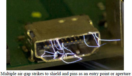
Some people may still have doubts, because the energy transfer did be seen when the ESD gun is simulated away from the object 1mm [20]. To further explain, this is only the effect of mutual capacitive/inductive coupling between the two conductors, and it does not include the arcing (flashover) effect of the humidity (water molecules) ionization in the air. The following image is taken from the Industry Council on ESD Target Level, White Paper Part II [10]
4.2 System ESD paper [8]
If you have been a senior EMC engineers for more than three years, or more than five years of senior hardware engineers, may have this experience: sometimes PCB seperated plane can enhance system ESD tolerance (for the PCB is usually under connector, and connected/grounded to the chassis), but sometimes it makes the system ESD and EMI worse. Why?
Refer to [8] guide of this paper , or next section 4.3 to validate these phenomena with simulation
4.3 System ESD simulation
4.3.1 ESD discharges to ground plane. Simulate by HFSS v15
When ESD discharges on ground plane, the plane with higher impedance (with slot or EBG pattern) will get better system ESD immunity. It is caused from the damping effect of plane impedance.
4.3.2 ESD discharge to a microstrip line. Simulate by HFSS v15
On the other hand, when ESD discharges on transmission line with discontinuous reference plane, it will get worse system ESD immunity. It is due to high frequency component of signal (as ESD energy) will get more ringing (reflection) for discontinuous transmission line.
Segmentation will increase the impedance of the plane path, which in theory will improve the ESD immunity, but if it makes the transmission line placed on different reference planes, the system SI/PI/esd/EMI will become worse as well. In addition, the ground plane segmentation changes the path of ESD discharging, and makes larger difference potential for the different areas, that is also the reason of the system ESD getting worse.
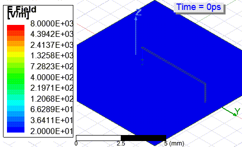
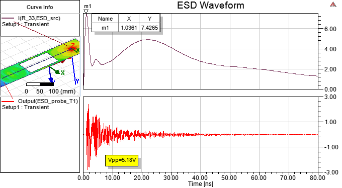
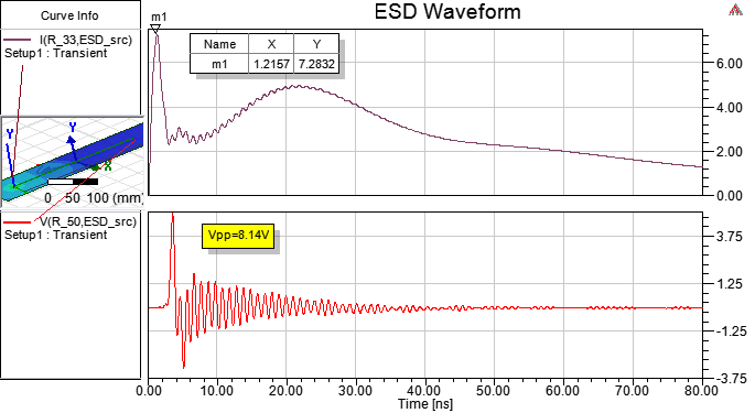
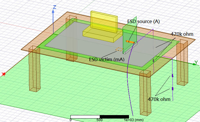
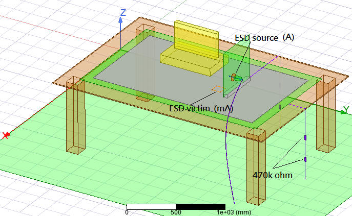
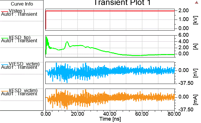
4.3.3 Vertical Indirect Discharge Simulation with 2019 R1 HFSS
4.3.3.1 Use ESD Gun from 3.1
|
|
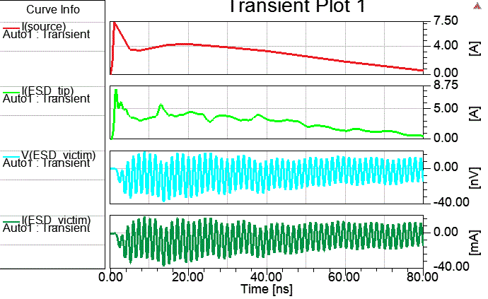
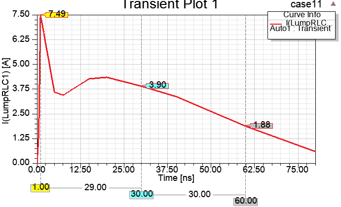
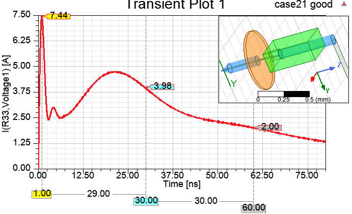
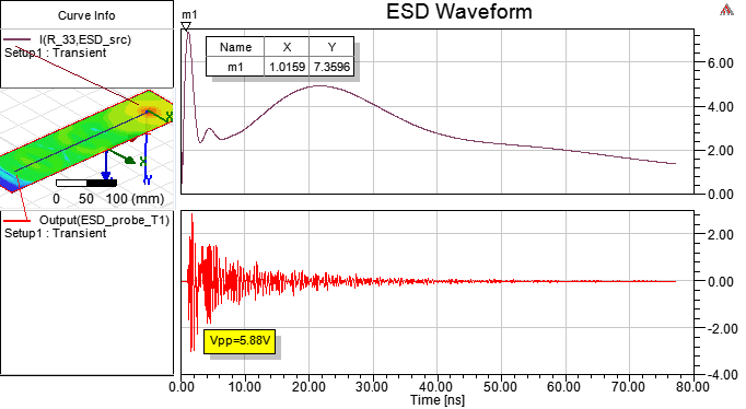
When the square metal ring (ESD victim) is awayfrom the vertical metal plate 0.1m (defined by IEC), the induced current/voltage peak on the metal ring is approximately 38mA/38nV.
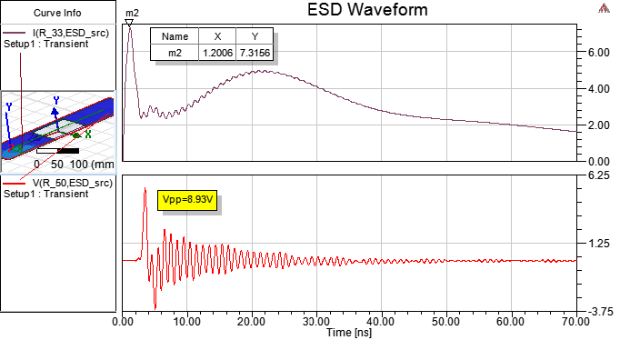
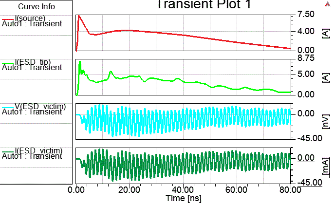
4.3.3.2 Use ESD Gund from 3.2

It is very close to 4.3.3.1, but the maximum of I(ESD_tip) is smaller than 4.3.3.1. This value (6A) is less than 7.5A, and I actually feels that it is a more reasonable result.
-
Q&A
5.1 Any relationship between IC and System ESD?
Ans:Reference [10] 2012 p.17, there is a comparison table Fig.1, and it claims the system ESD is independent from IC ESD. That is, even the immunity of IC ESD does well, it does not represent the system ESD will be good as well, becaue system ESD considers more factors. Please note that such arguments and comparisons are highly controversial : 1. This comparison is based on only HBM of IC ESD, not including MM, CDM, and IC latch-up performance. 2. It does not compare with the same system conditions/environment either. Try to imagine a situration, for low-level consumer products, to add one more 0.1uF capacitor are concerned very much, if the competitor's IC solution directly replaces yours on the same board, and gets better ESD immunity capability, can you still feel that there is nothing need to do for IC performance improvement? Therefore, this question should be asked in another way: under the same system design conditions , IC ESD and system ESD is directly related?
I fully agrees that "More factors need to be considered for system ESD immunity. To get the system ESD good, not just make sure the IC strong enough, FW robust, strong WDT (watch dog timer), system level PCB layout and components selected ... all of these are important. As long as you have a few years of actual IC mass production experience, it is not difficult to find a good IC ESD tolerance, it did help the IC market competitiveness absolutely. In further, only increasing IC ESD (including HBM,MM,CDM) and Latch-up capabilities with minimum IC costs addition, that can get competitive. Otherwise, it is just in the matter of debating which side (by IC or system) to cover EMS problem. The answer is simple, only the one who overcomes the problem gets the better profit. If you push the responsibility out, you are waitting to be eliminated.
Some people may still question my statement:IC ESD concerns IC damage, however system ESD concerns system function downgrade, they are different. Why did I say that they are related? Let's explain it from how the ESD protection circuit work inside the IC die level. In fact, it is also all about the venting of noise (RC push MOS transient path), clamping voltage ...ect. , the same concept as system protection. If the system ESD is not good enough, there may be system function downgrade, or IC function downgrade. When the different models encounter problems in mass production, you don't know which one is the system dominate, which one is the IC dominate, so both of them should be taken care well.
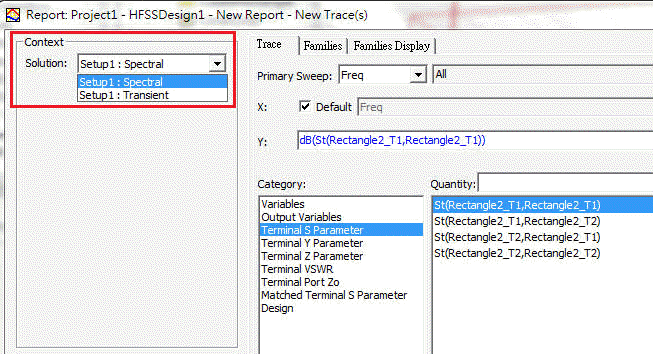
5.2 How to plot S-parameter under Transient mode?
Ans:Only "Transient" solve + "Network Analysis" can plot S-parameter from [Report Rectangular] with [Spectral] solution setting.
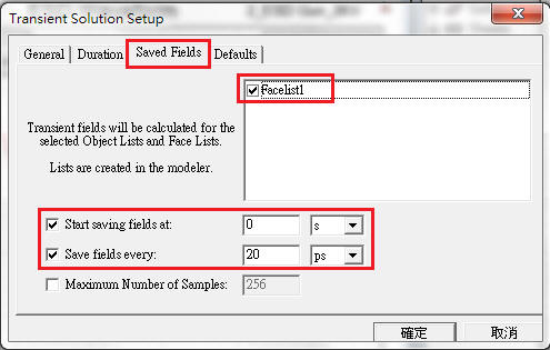
5.3 How to plot Field result for transient solve?
Ans:To plot the field of transient analysis, some setting have to be done first
-- select surfaces, and add list from [Modeler\ List\ Create\] to plot fields result
-- set "save field" in setup window
5.4 Can lump RLC boundary be used on a solid object?
Ans:For HFSS frequency domain, it is ok, but for time domain solve, it permits "rectangle" sheet only for "Lump RLC boundary"
5.5 Can HFSS simulate CDM(Charge Device Mode) ESD?
Ans:HFSS can't simulate CDM alone, because HFSS can't charge Q(charge) to nonconductor. However, HFSS+Circuit model can do it [21].
CDM is that a lot of static charge accumulates on a device (the entire device of non-conductor + conductor, such as package) first, and discharges to the nearby conductor. It causes a large current flowing from the charged body itself instantaneously and damage the device.
5.6 What differences are between the 3 kinds of HFSS ESD Gun?
Ans:The method of section 2.1 is established by the concept of two-stage discharge of arms and body. It's behavior is similar to section 2.2 [3][4], and Ipeak appears fast and sharp. Althought the method of sec. 2.3 has been cited in the IEEE many times since 2003 ([2][6][7] the same batch of research teams), but it's Ipeak appears slower and thicker.
5.7 What factors will affect the speed of HFSS Transient Solver?
Ans:
There are two processes for transient analysis, one is the mesh and the other is the transient sweep. The time of former one is related to the size and complexity of the 3D geometry, however the time of latter one is related to the characteristics of the energy field changing with time. For the problem of intense energy changes in a short period (a broadband problem), because it requires a smaller time step, the transient sweep time will be longer.
For HFSS transient analysis, the delta error can be set from 0.1 to 0.01, and the smaller the value, the longer the simulation time. I am used to making refine mesh at least 3~5 times to avoid oscillations of time domain (not converged).
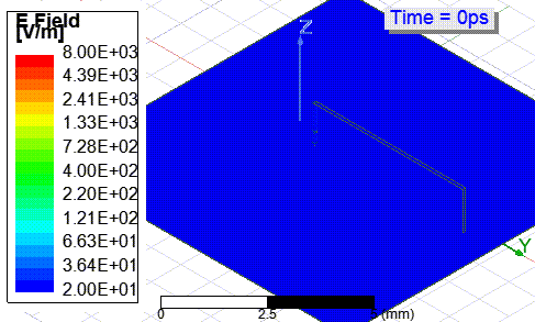
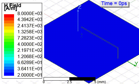
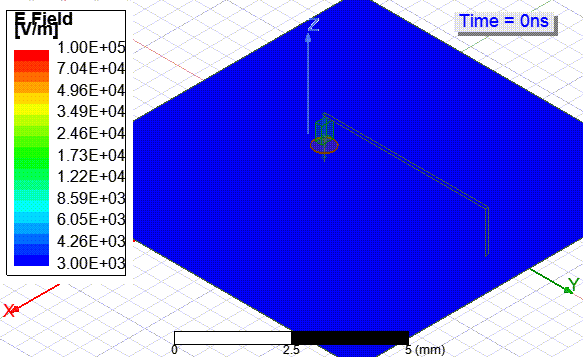
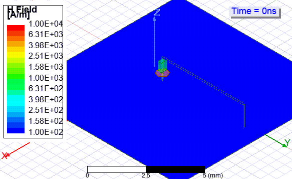
5.8 To observe voltage/current of ESD, should we check E-filed or H-field?
Ans:Where the voltage (drop) is larger, the electric field is stronger as well, and the flow of charge produces a magnetic field. So we look at E-field for ESD voltage distribution, and look at H-field for ESD current distribution.
Seeing the distribution of voltage bright spots and the distribution of current bright spots have different meanings, and whether the system components die in overvoltage (EOS) or overcurrent (ESD) is another problem. In general ESD testing, component damage (Class D) is often caused from the transient overcurrent breaks down the IO, or the ESD triggers the Latch-up in the CMOS IC to damage the IC.
5.9 When ESD discharge, the grounding end of ESD gun strap will shine or not?
Ans:When performing ESD simulation with 3D EM tool, and looking at E-field, there is only a bright spot at ESD tip end. However, if you look at H-field, both of the discharge end and the ground end have bright spots.
In the HFSS, no matter which method to implement ESD gun model, when doing system ESD simulation, it will be seen that while ESD gun is discharging (at 1 ns), there is also a current flowing from ESD gun through the ground strap to the reference ground (at 1ns~7ns). The reason is:a real ESD gun charges the 150pF capacitor by a relay/DC voltage and discharge with a two-stage model. In the FEM environment, the front switch (V114) in the equivalent circuit of 2.2 directly replaced by a 2KV step waveform, which causes the voltage at one end of C3 (150pf) to be pulled up instantaneously, and the voltage at the other end of C3 is also pulled high, that causes a current flowing on the ESD strap.
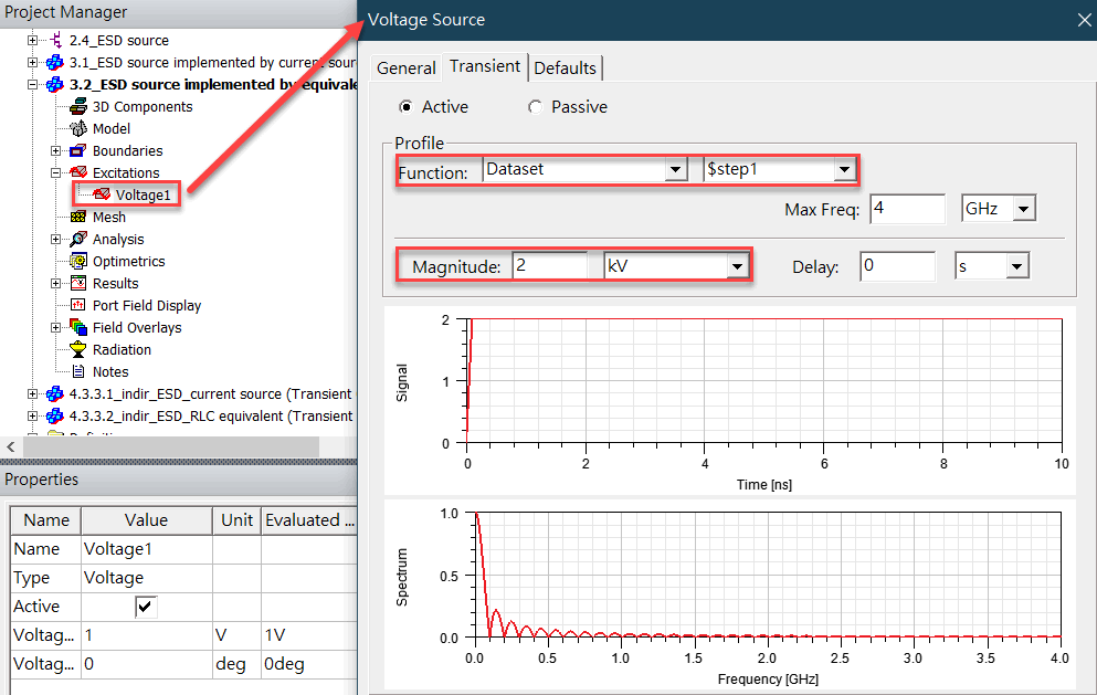
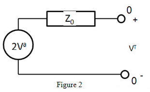
5.10 What is the difference between Lump Port or Voltage Source for Transient solver?
Ans:HFSS Help says that transient analysis works with Wave port, Lump port, Voltage source, Current source and Incident wave, and the simulated result of voltage source defined by dataset is the same as that of Designer circuit. However the result of driven terminal lump port defined by the same dataset will be obviously larger than voltage source.
For more information on this issue, see the [Excitations in Time Domain] in the HFSS Help. Figure 1 below shows how does the transient simulation of the driven terminl lump port work. By Kirchhoff's voltage law, the circuit is equivalent to the Figure 2, which is the way voltage source and circuit simulation engine approach. So, if you use Terminal Port (as lump port in driven terminal) in HFSS Transient, the input voltage defined by dataset should be *0.5 volt.
One needs to be careful when comparing results with a circuit tool or textbooks using the voltage source shown in Figure 2. If one volt is used for the voltage source in the circuit simulator, this should be compared with a HFSS transient simulation with edit sources set to 0.5 volt. |
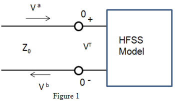
By the way, lump port must be connected to the Lumped RLC boundary through Perfect_E to catch the terminal, while the Voltage Source does not.
If the original design with lump port is copied and change to voltage source excitation, the "Max. DeltaEnergy" seems to automatically change from 0.01 to 0.1.
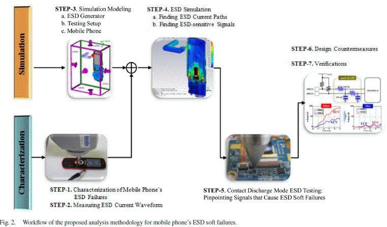
5.11 How to detect ESD soft failures (Class B) and find the root cause to improve?
Ans:Samsung published an IEEE Transaction paper [9] in 2011. As I said earlier, the key point of EMC simulation is that it is necessary to narrow-down check for converging the problem first by system analysis (as Step 5 or the figure below), then model the problems and try to reproduce EMC issues by simulation.
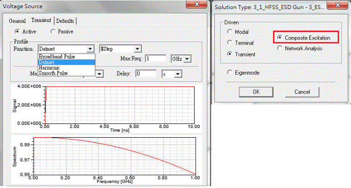
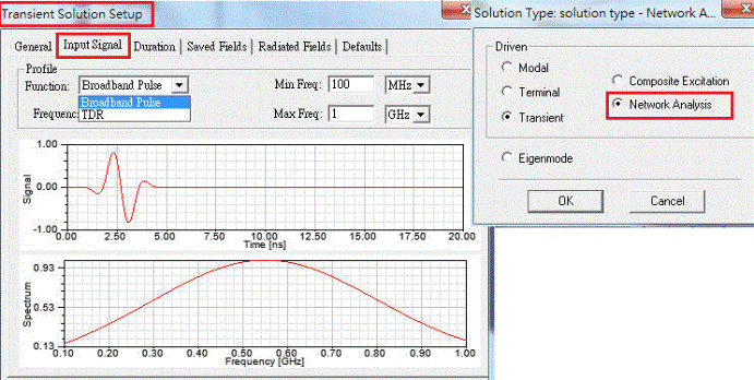
5.12 What is the difference between Composite Excitation and Network Analysis of Transient solver?
Ans:
5.12.1 For "Composite Excitation", different ports can have different excitation sources. The type of excitation sources can be set separately in the Excitation property (which can be defined differently from each other), and are calculated simultaneously in the simulation.
5.12.2 For "Network Analysis", all excitation sources are the same. The type of the excitation source is moved to the Solution Setup as below and set up with the same excitation definition.
5.13 ESD gun is charged by a voltage source, however the discharge tip waveform is defined by voltage or current?
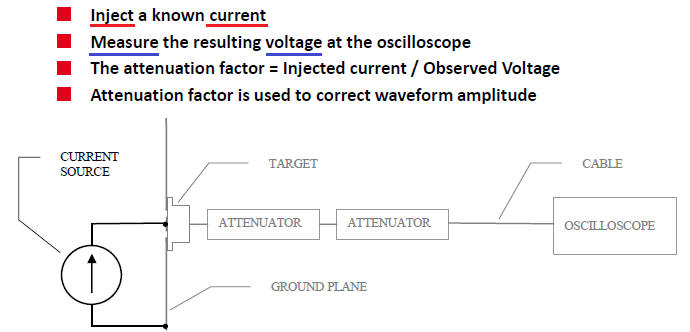
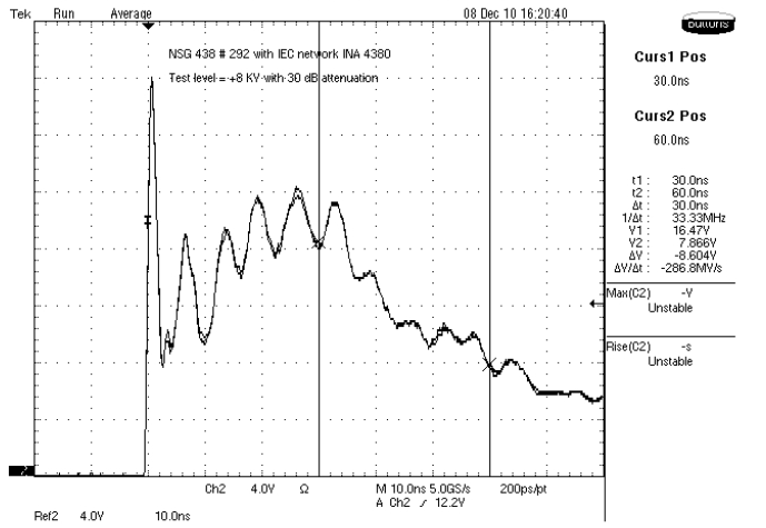
Ans:ESD gun outputs a current pulse (current source), and the regulation defines the current waveform of discharging too (as defined in section 1.1). However, when the instrument manufacturer or measurement center is doing the ESD Gun calibration, in fact, they directly measure voltage through the attenuator by the oscilloscope. The current pulse is attenuated by 30dB and enters the oscilloscope to measure the rise time [14].
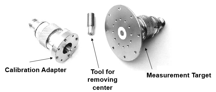
The TARGET in the above picture is a very important device. It looks like the picture below. The middle is the current output point and is surrounded by a circle of grounding points. It is a coaxial connector.
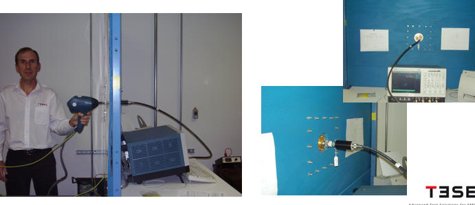
The configuration of the test system is shown in the figure below:ESD gun output is transmitted to the TARGET, and it is connected to the oscilloscope through a attenuator.[14]
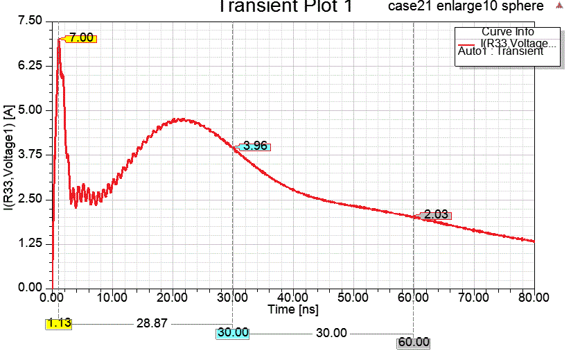
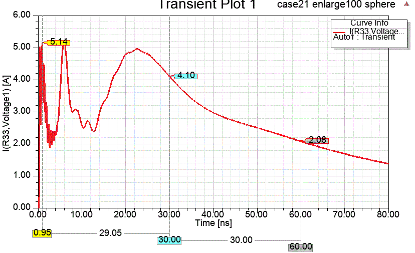
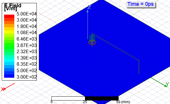
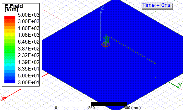
5.14 What is the impact of the modeling size of the ESD simulation environment (including ESD gun /ground strap)?
Ans:
The 3D size of ESD system simulation in step3 is very small, only about 7mm*7mm*7mm, so looking at the H-field. You will see ESD gun tip and the ground strap grounding point almost light at the same time, and don't see how the current flows in the ground strap. As long as you try to re-scale from mm to meter (10 to 100 times magnification), you will observe the phenomenon of energy spreading over time.
When the 3.2 ESD Gun unit is magnified 10 times (re-scale from mm to cm), the first peak of the ESD current profile drops and the waveform will carry a ringing, which is mainly due to the increase of the impedance and inductance of the entire discharge loop.
| 10x times scaling | 100x times scaling |


Reference [3] has a very nice table:
5.15 What is the spectrum of ESD effect? Is it 300M~1GHz?
Ans:No.
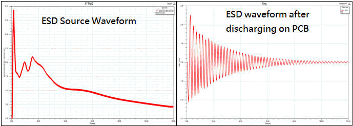
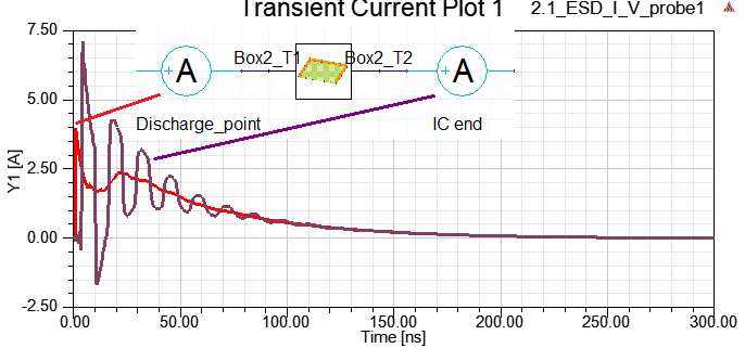
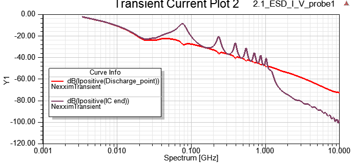
First, the spectrum of ESD source waveform and the one that ESD discharg on PCB are different.
The second point:the spectrum of ESD discharge energy is wideband. We can clearly understand the matter from the simulation results and 2010 IEEE paper [15].
Therefore, the bypass capacitor (decoupling capacitor) is not an effective ESD protection component. Good ESD protection components should be able to quickly vent current noise from very low frequencies to high frequencies (hundreds of MHz) and contribute minimal parasitic effects to the protected circuit. So, I do not think and don't know why someone said ESD is a 300M~1G noise.
2010 IEEE paper [15]
Take 2.1 example of this article (with 1.1KV), ESD source waveform and spectrum simulation results as below
5.16 For the same structure, why it gets no E/H field after changing discharge waveform from 80~100ns to 80~100ms?
Ans:
Although the same structure, when the input wavelength becomes 1e+6 times larger, the electrical size equivalent of this structure becomes 1e-6 times smaller. For HFSS time domain solver, in the face of such special condition (very small electrical size and low energy transfer close to DC), the recommended practice is to use zero-order with solver inside.
5.17 Is there a successful case of system ESD failure analysis from IC to board end? It is better to have a simulation and measurement comparison.
Ans:Following the first paper about ESD fast analysis of PCB board system using HFSS from Korea Ulsan University in 2017 [16], it further analyzed the complete ESD circuit failure from IC circuit to system PCB with HFSS and HSPICE [17] in 2019.
A very good practical paper, without an arduous theoretical basis, is to just honestly simulate and measure IC circuits and the parasitic effects of systems. A seemingly simple paper is so far the best and most complete system-level ESD failure analysis that I have seen (you can see how the logic gate in the IC is affected by ESD noise).
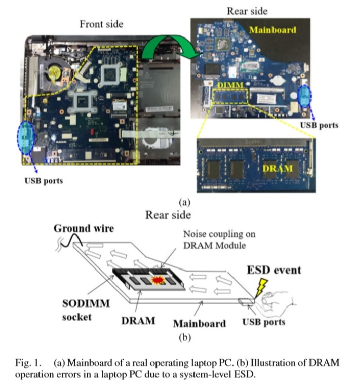
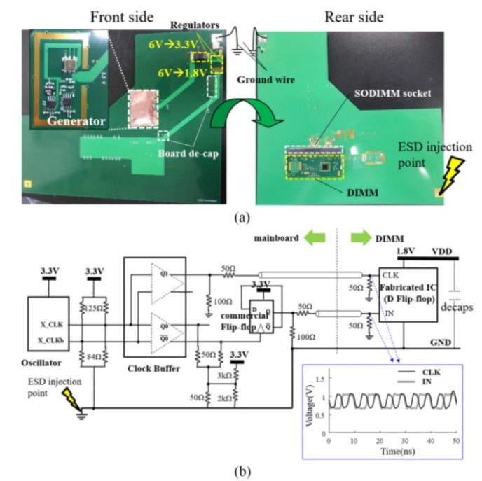
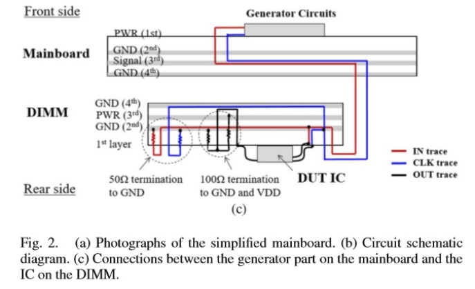
- The original system (notebook) board, ESD immunity test on USB connector will cause DRAM failure
- Simplified circuit board and test IC for simulation and measurement (by CLK and D flip-flops). Even simplifying, the key characterics such as the PCB size, layout placement, and the socket connection between the motherboard and the DIMM daughter board, ...etc., are maintained to ensure the accuracy is good enough to distinguish the performance from different ESD strategies.
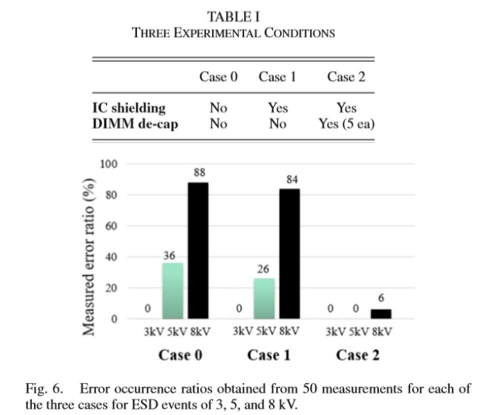
- Compare case1, case2 (with solution) to case0 (original),50 times of ESD immunity testing
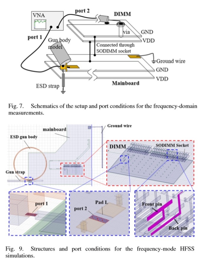
- HFSS model
- Compare HFSS simulation with measurement
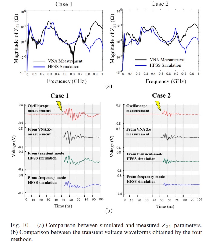
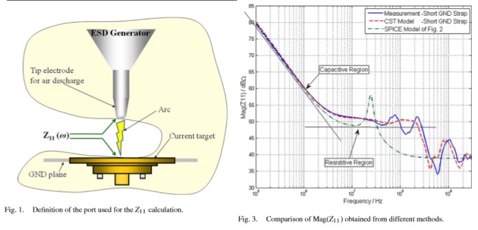
5.18 This article 4.1 emphasizes that full-wave EM solver cannot be used for air discharge ESD. Why did an IEEE journal paper do this in 2011?
Ans:
The paper[20] first extracted the entire discharge path model with a full-wave electromagnetic field solver, and verified its Z11 with measurement and SPICE models.
The key point is that its SPICE equivalent circuit model defines a time-varying resistor R_arc (Fig2 in paper) as the basis for simulating air discharge behavior. In other words, air discharge simulation can not be achieved by a full-wave solver alone, an equivalent circuit model R_arc must be used.
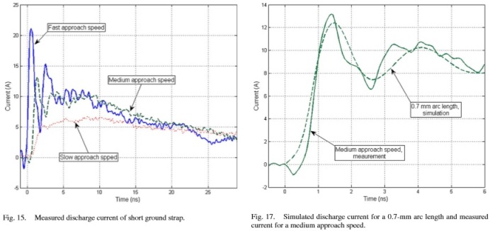
Next, the ESD gun was placed at three distances of 0.3mm/0.7mm/1.1mm, and compared the discharged waveform seen at the receiving end with the measurement. It is worth mentioning that, the speed of the ESD gun closes to the object is compared to the different air discharge distances in the simulation.
[1] IEC-61000-4-2 or EN-61000-4-2
[2] K. Wang, D. Pommerenke, "Numerical Modeling of Electrostatic Discharge Generators", IEEE Trans, Electromagn. Compat., 2003. (推薦)
[3] F. Centola, S. Caniggia, "ESD Extraction Model for Susceptibility Study", 2003
S. Caniggia, F. Maradei, "Circuital and Numerical Modeling of Electrostatic Discharge Generators", 2005. (推薦)
S. Caniggia, "Circuit and Numerical Modeling of Electrostatic Discharge Generators", 2006.
S. Caniggia, "Numerical Prediction and Measurement of ESD Radiated Fields by Free-Space Field Sensors", 2007.
M. Borsero, S. Caniggia, "A New Proposal for the Uncertainty Evaluation and Reduction in Air Electrostatic Discharge Tests", 2008.
[4] 邱冠銘, "Simulation and Measurement of ESD Test for Electronic Devices", 中山大學碩士論文, 2004 (推薦)
[5] "Modeling the Susceptibility of Enclosures to ESD and the Effect of Attaching Cables". CST, 2012
[6] J.koo, Q.cai, "Frequency-domain measurement method for the analysis of ESD generators and coupling", IEEE Trans. on Electromagn. Compat., 2007.
[7] F. zur Nieden, D. Pommerenke,"A Combined Impedance Measurement Method for ESD Generator Modeling", EMC Europe, 2011
[8] D. C. Smith, Ed Nakauchi, "ESD Immunity in System Designs, System Field experience, and effects of PWB layout", EOS/ESD Symposium Proceeding, 2000 (推薦)
[9] K. H. Kim, Y. Kim,"Systematic Analysis Methodology for Mobile Phone's Electrostatic Discharge Soft Failures", IEEE Trans. on Electromagnetic Compatibility, 2011. (推薦)
[10] System Level ESD Part I : Common Misconceptions and Recommended -- 2010
System Level ESD Part II : Implementation of Effective ESD Robust Designs -- 2012[11] Characterization, modeling, and design of ESD protection circuits (book)
[12] Jing Li, Jun Fan, "The Application of Spark gaps on Audio Jack for ESD Protection", IEEE EMC Society, 2013. (推薦)
[13] R. Myoung, "Chip-Package-System ESD Simulation Methodology with Chip ESD Compact Model", DesignCon2014. (推薦)
[14] Greg Senko, "ESD Simulator Verification", p.34,48, EMC Society 2010
[15] Janusz Baran and Jan Sroka, "Distortion of ESD Generator Pulse Due to Limited Bandwidth of Verification Path", IEEE Trans. Electromagn. Compat.,2010.
[16] Junsik Park, Jongsung Lee, "Fast and Accurate Calculation of System-Level ESD Noise Coupling to a Signal Trace by PEEC Model Decomposition", IEEE Trans. Electromagn. Compat.,2017.
[17] Myungjoon Park, Junsik Park, "Measurement and Analysis of Statistical IC Operation Errors in a Memory Module Due to System-Level ESD Noise", IEEE Trans. Electromagn. Compat.,2019. (推薦)
[18] Ahmad Hosseinbeig, Omid Hoseini Izadi, "Methodology for Analyzing ESD-Induced Soft Failure Using Full-Wave Simulation and Measurement", IEEE Trans. Electromagn. Compat.,2019.
[19] Darwin Zhang Li, Shubhankar Marathe, "Full-Wave Simulation of System-Level Disruption During Secondary ESD Events in a Smartphone", IEEE Trans. Electromagn. Compat.,2019.
[20] Dazhao Liu, Argha Nandy, "Full-Wave Simulation of an Electrostatic Discharge Generator Discharging in Air-Discharge Mode Into a Product", IEEE Trans. Electromagn. Compat.,2011.
[21] Dolphin Abessolo-Bidzo, "CDM Simulation Based on Tester, Package and Full Integrated Circuit Modeling: Case Study", IEEE Trans. on Electron Device, 2012.
[22] CDM Circuit Model