線上影音
Home > ANSYS SIwave教學> DDR SI+PI Co-simulation
This article is intended to introduce how to do SI+PI co-simulation with SIwave v5.0+Designer v6.
-
問題與討論
7.2 What is the difference between Touchstone and SPICE model for PCB?
7.3 Why is U503 PI worse than DDR500 device in time domain (as step6.3 result)?
7.4 Why are the DC voltage of P1.5V and P1.5V_AUX more than 1.5V in step 4.2.4?
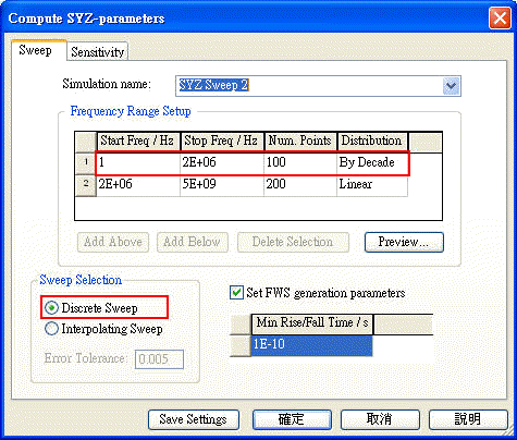
7.5 Compute more frequency points with discrete sweep and run step4、step5 again.
![]()
1.1 It is interesting that there is different PDN net of DDR3 in the project:BGA(U503) uses P1.5V and DDR3 device (DDR500) uses P1.5V_AUX, and some 0.1uF capacitors straddle between P1.5V and P1.5V_AUX.
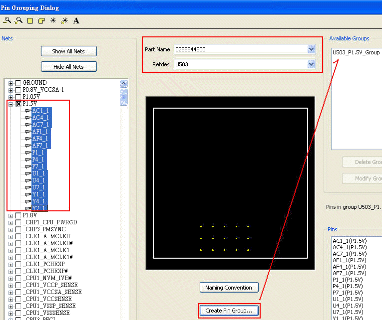
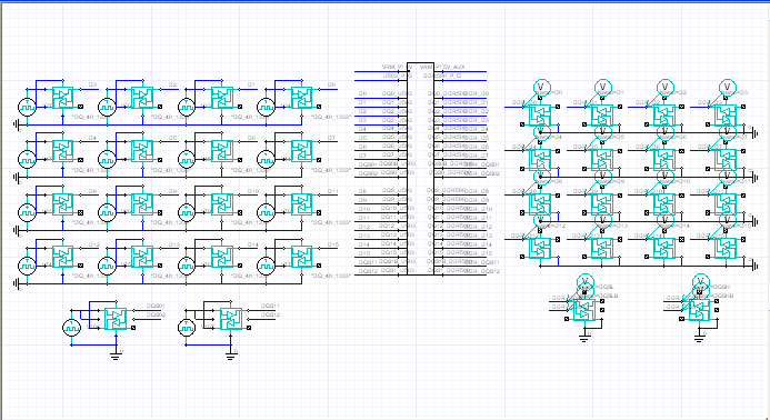
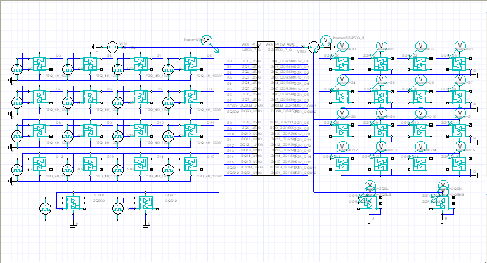
1.2 Add all ports for DDR3 D0~D15, DQS0, DQS0B, DQS1, DQS1B, U503 P1.5V, DDR500 P1.5V_AUX, and VRM
1.2.1 Add all Data and DQS port
1.2.2 Use [Tools \ Pin Group Manager] to generate P/G pin-group of U503 and DDR500 devices
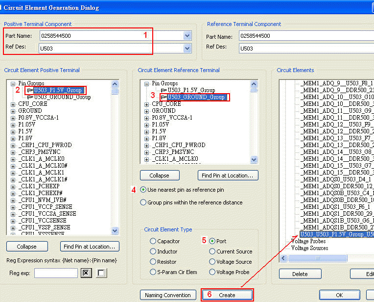
1.2.3 Use [Circuit Elements \ Generate on Components ] to generate P/G ports of U503 and DDR500 devices
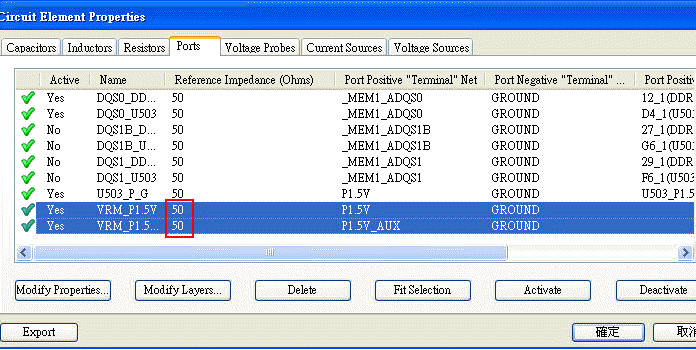
1.2.4 Add port VRM_P1.5V、VRM_P1.5V_AUX for U503 and DDR500
Use 0.1 ohm for VRM reference impedance, not 50 ohm
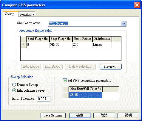
1.3 Run [Simulation\Compute S-,Y-,Z-] to extract S-parameter
1.4 Export to Touchstone or SPICE file
Results \ SYZ \ SYZ Sweep1 \ Export to TouchstoneR File (.snp) or
Results \ SYZ \ SYZ Sweep1 \ Compute FWS sub-circuit (means Full-wave SPICE model, .sp)
2.1 Download Micron DDRIII-1600 IBIS
2.2 SI simulation, that is, IO models use default (ideal) power
2.3 SI+PI simulation, that is, IO models use non-ideal power
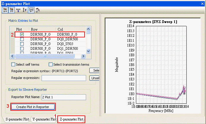
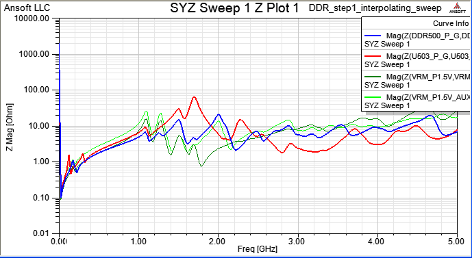
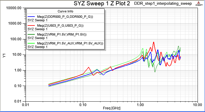
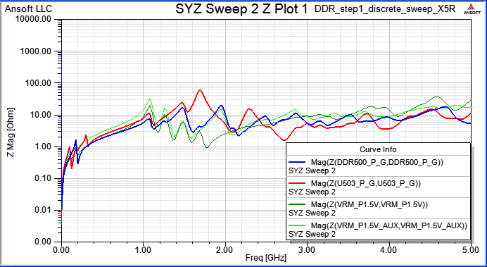
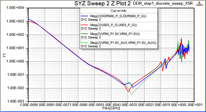
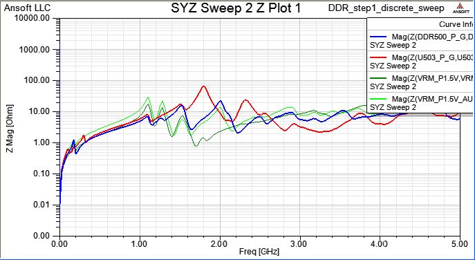
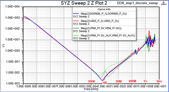
4.1 SIwave Z-profile (target impedance check):Results \ SYZ \ SYZ Sweep1 \ Plot Magnitude/Phase
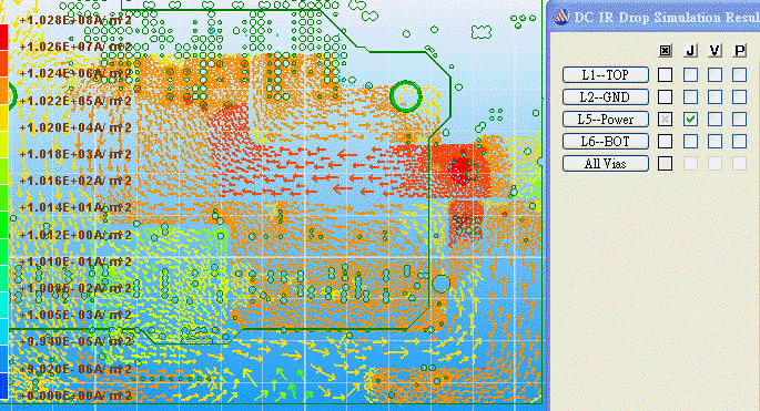
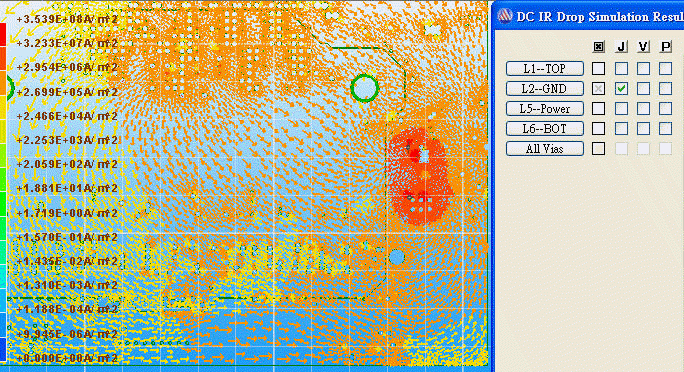
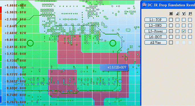
4.2 SIwave IR drop check:
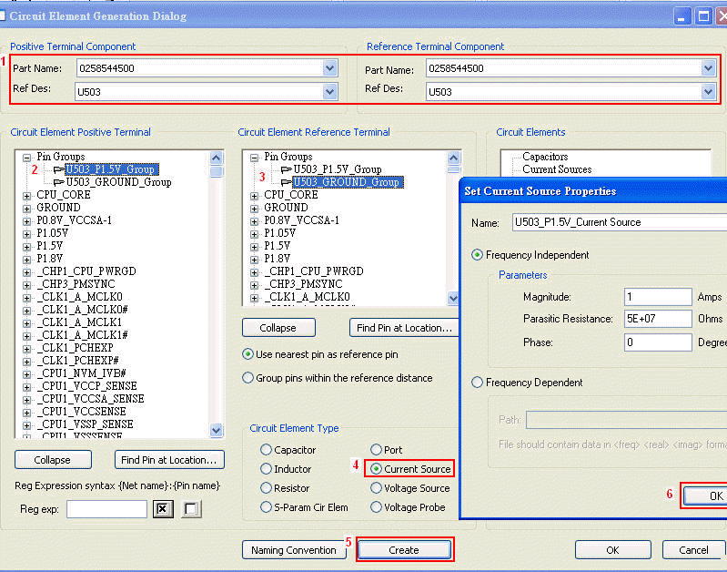
4.2.1 [Circuit Elements \ Generate on Components ] to generate [Current Source] for U503
4.2.2 [Circuit Elements \ Voltage Source] to add two [Voltage Source] 1.5V for VRM_P1.5V、VRM_P1.5V_AUX
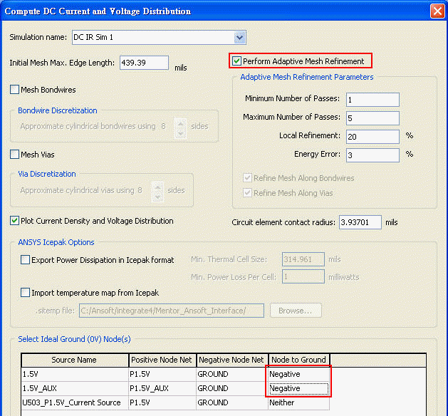
4.2.3 Run [Simulation \ Compute DC Current/Voltage]
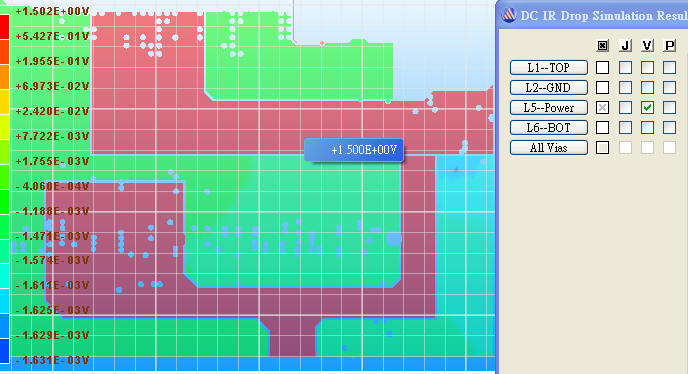
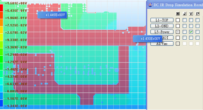
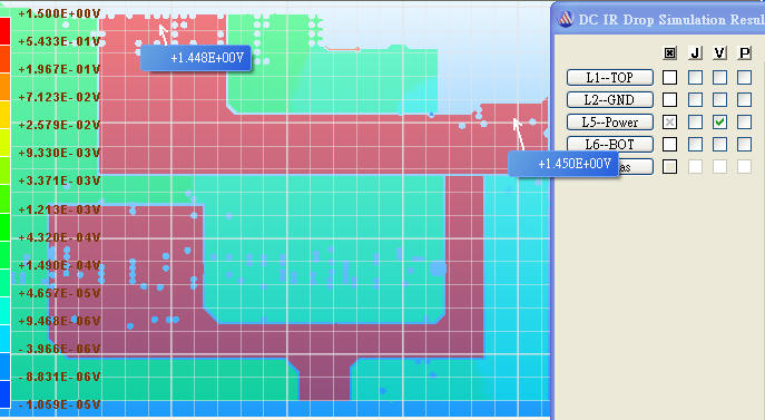
4.2.4 [Results \ DC IR Drop \ DC IR Sim1 \Currents/Voltages]
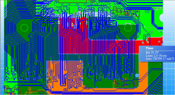
Power plane current distribution
GND plane current distribution
Power plane voltage distribution
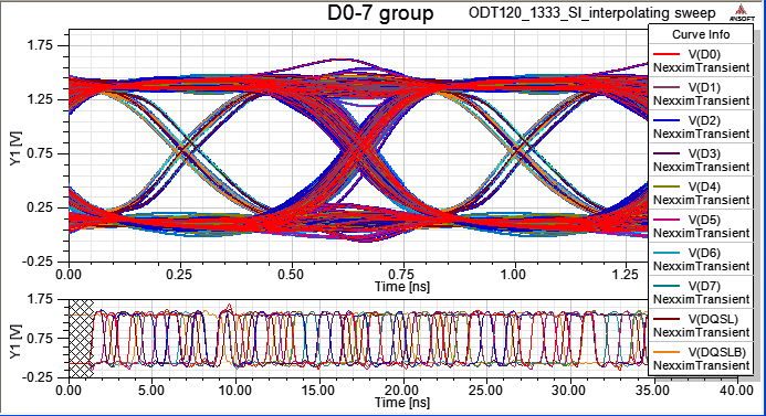
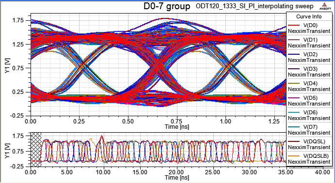
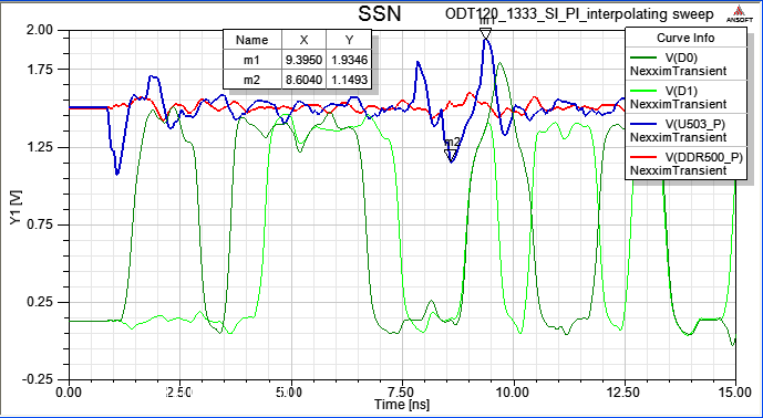
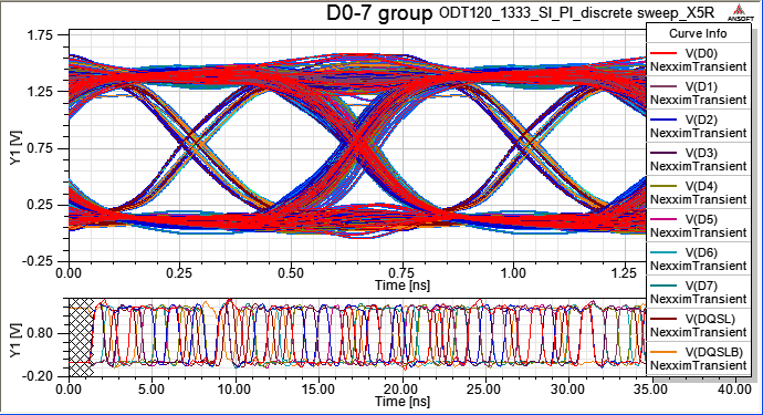
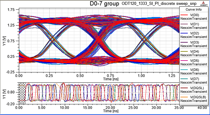
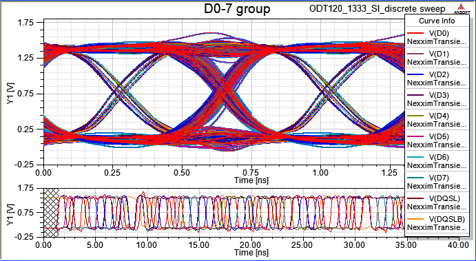
5.1 Compare to step3, the eye waveform in step5 is more worse.
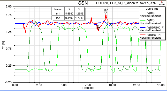
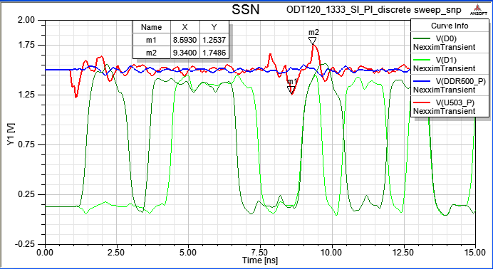
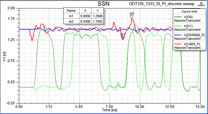
5.2 Power integrity of U503 is more worse than DDR500 device, and the SSN of U503 is about Vpp=0.7V.
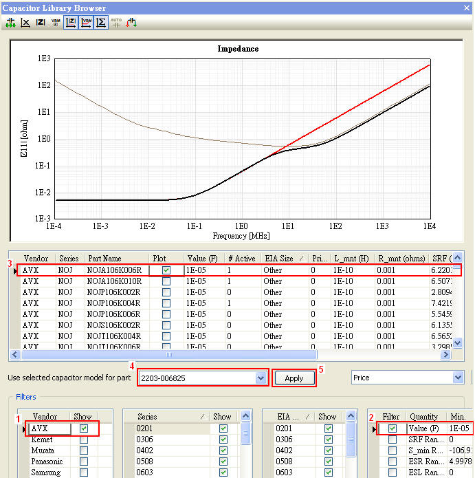
6.1 Use AVX 10uF model for C430、C431、C433、C434、C436、C437、C467、C469、C470、C473、C475、C476
Tools \ Capacitor Library Browser
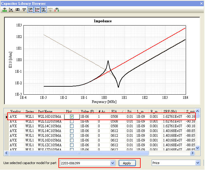
6.2 Use AVX 1uF model for C468、C471、C472、C474
6.3 Compute SYZ-parameter again and compare the result to step7.5.3
- 問題與討論
7.1 IO使用IBIS或SPICE model會差多少?
Ans:SPICE IO model的波形會比IBIS準確Ansoft document p.9,而有一篇conference則是說把IBIS加上適當的寄生電容值(on-chip decoupling capacitor)效應後,則兩者可做到非常接近。如果要做SI+PI co-simulation,建議盡可能用SPICE model,其次是用IBIS 5.0 (power aware)。
7.2 What is the difference between Touchstone and SPICE model for PCB?
Ans:對於plane較完整的簡單結構,兩種模型都可以,跑出的結果也一樣;但對於plane較複雜的結構,建議用S-parameter(.snp)較易處理收斂問題。原因是SIwave原始分析出來的資料是S參數,轉成SPICE RLC model可能會產生model reduction轉換失真。如果要用SPICE model來表示PCB,那也請使用full-wave SPICE model
In general, using touchstone (.snp) file directly can avoid model reduction.
For this case, using SIwave v5.0 and SPICE model (.sp) can get the same result as using touchstone (.snp) file.
7.3 Why is PI of U503 more worse than DDR500 in time domain (as step6.3 result)?
Ans:The Z-profile of U503 and DDR500 are alike, and the root cause leading to worse PI for U503 is that the role of U503 in PDS is drive output buffers, but role of DDR500 is input terminals. U503 is the one with more power consumption.
7.4 Why are the DC voltage of P1.5V and P1.5V_AUX more than 1.5V in step 4.2.4?
There are three methods to get better result, but just one method is right.
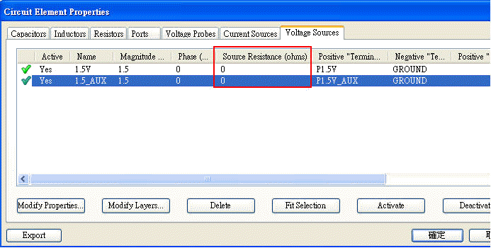
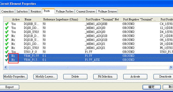
7.4.1 Modify source resistances of voltage P1.5V and P1.5V_AUX from 0.05 to 0
7.4.2 Keep source resistances of P1.5V and P1.5V_AUX 0.05 ohm, but modify VRM reference impedance from 0.1 to 50 ohm
7.4.3 De-active ports of VRM_P1.5V and VRM_P1.5_AUX, and keep source resistances of P1.5V and P1.5V_AUX 0.05 ohm. The source terminal of P1.5V = 1.5-0.05(ohm)*1(A)=1.45V
Reference impedance of port理論上不應該影響到我們做IR drop的模擬,但實驗結果顯示還是關掉的好 。參考Ansoft官方做IR drop的模擬教案,也是只有放voltage與current sink,沒有任何port。Please refer to SIwave\Power Integrity 6.6
7.5 Compute more frequency points with discrete sweep and run step4、step5 again.
7.5.1 Select [Discrete Sweep] sometimes can fix non-causality and non-passivity problem, but refer here for a better way.
7.5.2 SI simulation result is the same as step3.
7.5.3 Z-profile is different to step4 in low frequency (1~50MHz).
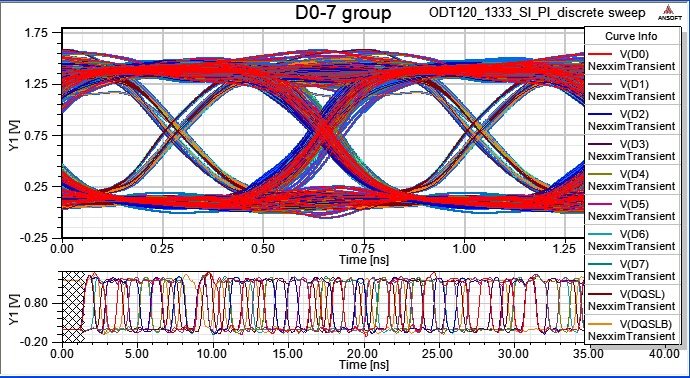
7.5.4 SI+PI simulation result is more better than step5.1.
7.5.5 The simulation result is more better than step5.2, SSN Vpp=0.5V
-
[1] Accurate and Efficient SSN
[2] "Mixed-Reference for Optimum Cost & Performance in High-Speed Memory Interface", DesignCon2014.
