線上影音
Home > ANSYS SIwave教學> PI Optimize II
The article (part II) is intended to introduce a novel method using "PI Advisor" in SIwave v5.0. (refer to Ansoft 2010 presentation)
-
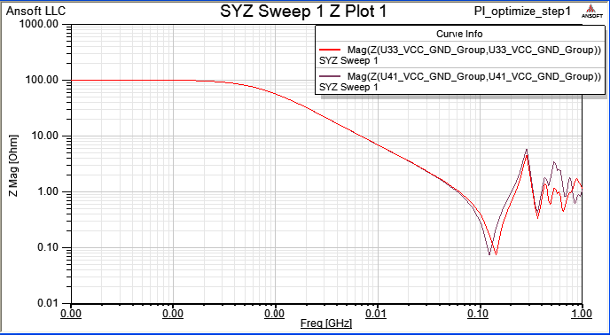
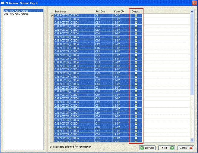
Original Design with VCC to GND 54 Capacitors (100uF+0.1uF)
-
問題與討論
5.1 Step4.5 shows that optimized result can't meet specification:1 ohm from 500MHz to 2GHz. why and how to do better?
5.2 Why does step4.2 keep C9, C10 100uF, not optimize them?
5.3 Is there any special function in PI advisor? -
總結
PS:PDN (Power Distribution Network),PDS (Power Distribution System)
![]()
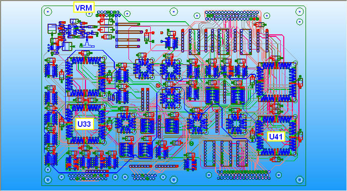
1.1 Following PI_Optimize_I step1, create pin group and grouping port for VCC of U33 and U41
1.2 The bare board Z-profile
-
Original Design with VCC to GND 54 Capacitors (100uF+0.1uF)

2.1 Following PI_Optimize_I step4, create pin group and grouping port for VCC of U33 and U41
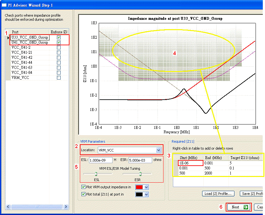
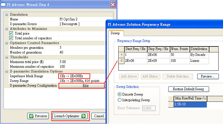
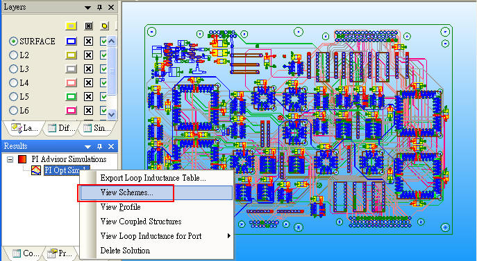
4.1 SIwave \ Simulation \ PI Advisor
Define target impedance, |Z11| profile and VRM for each ports individually.
Set start frequency of required |Z11| to be 1Hz, not 0Hz. Otherwise, optimized result will almost use large capacitors.
4.2 Select all capacitors, except C9,C10 to be optimized
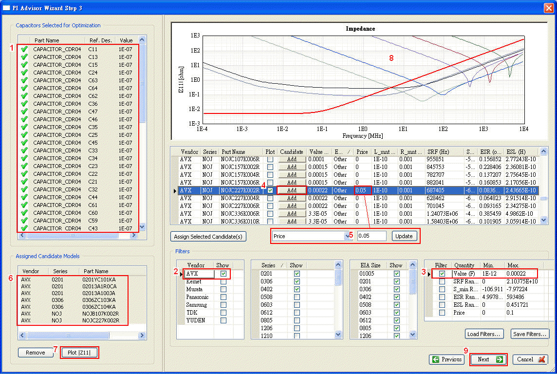
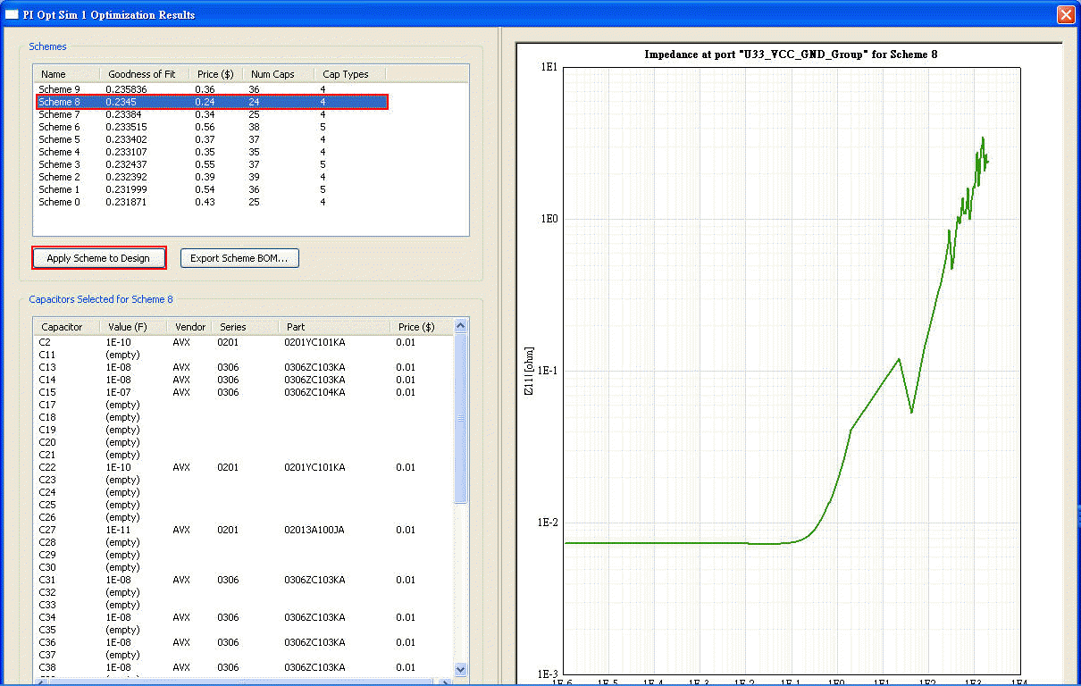
4.3 Select all capacitors to be optimized, and select 220uF、100uF、0.1uF、10nF、100pF、10pF、1pF to be used.
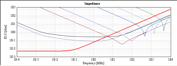
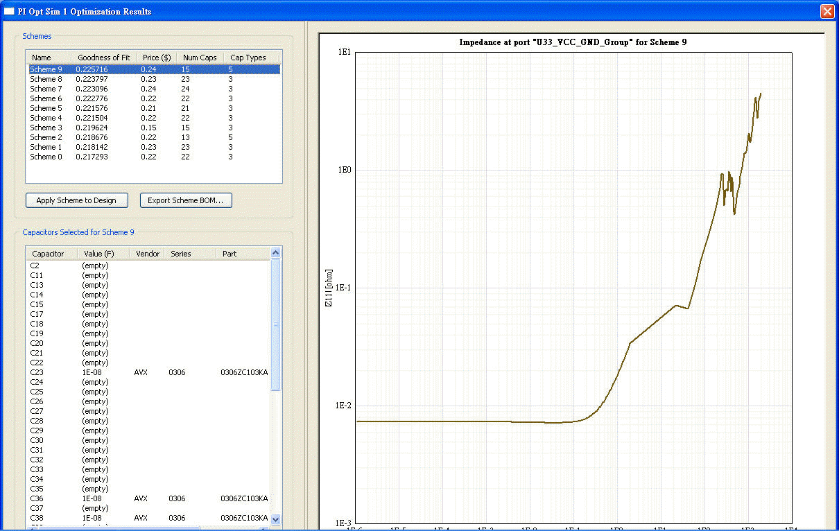
4.4 View PI Optimized Result
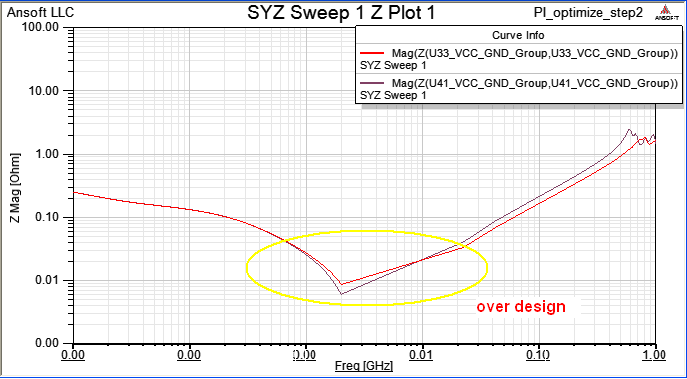
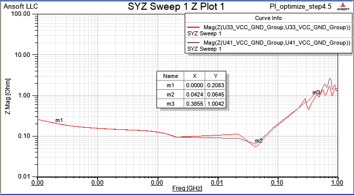
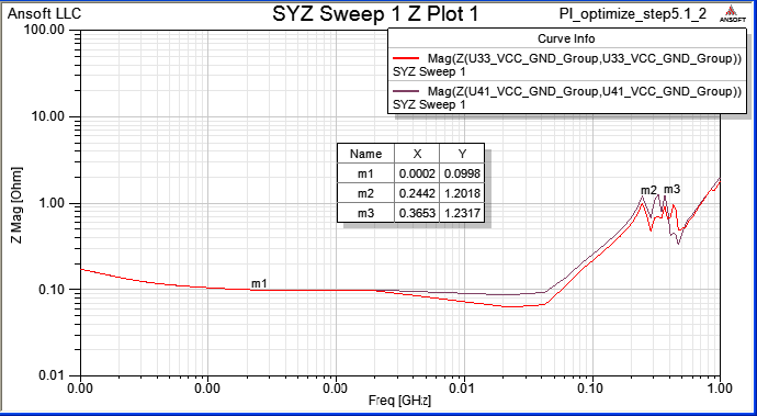
4.5 [Apply Schematic Design] and Compute SYZ-parameter again, the Z-profile as below
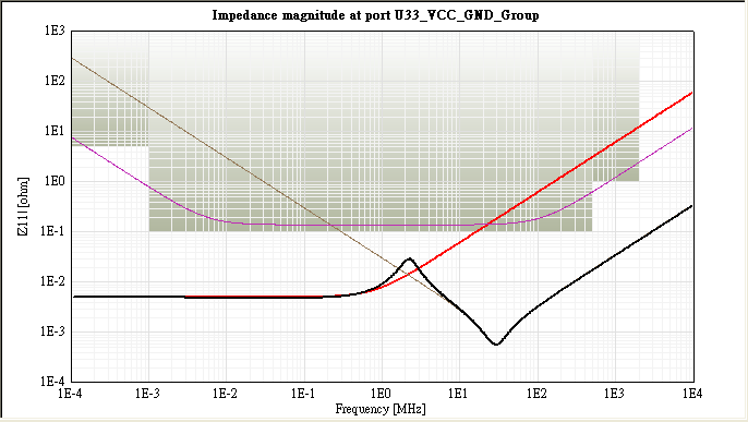
5.1 Step4.5 shows that optimized result can't meet specification:1 ohm from 500MHz to 2GHz. why and how to do better?
Ans:To reduce PND impedance from 400MHz to 1GHz, high-frequency decoupling capacitors have to be placed nearby IC pin, and allocate bulk cap./HF cap. suitably. Let's assign 100pF to four more capacitors (C6,C7,C8,C12) (C1,C3,C4,C5), and 0.1uF to (C38,C39,C49,C50,C53) (C47,C62,C63,C64) around U33、U41 manually.
Totally 15+8=23 capacitor.
5.2 Why does step4.2 keep C9, C10 100uF, not optimize them?
Ans:C9、C10是VRM input,這位置限制放大電容,目的是為了穩住電壓源頭。也可以在step4.2中把C9、C10核選,但在step4.3中,指定C9、C10只能套用100uF或220uF的大電容。5.3 Is there any special function in PI advisor?
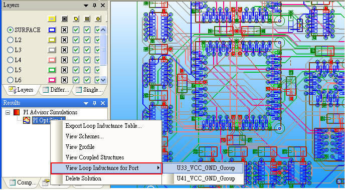
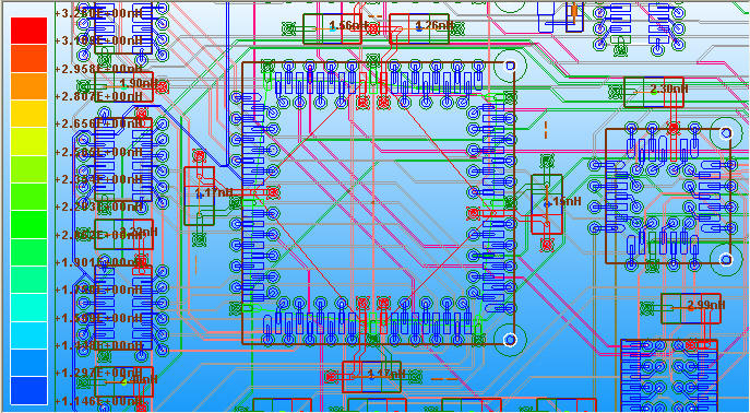
上圖中的C6、C7、C8、C12若在step4.2沒有指定被optimize,此功能就不會去計算loop inductance
-
PI Advisor for Optimized DDR3 Memory Design by Ansoft 2010.12