線上影音
Home > ANSYS SIwave教學> DDR SI Simulation
本文始於2011.12,旨在為學習過SIwave \ Lesson 17的讀者,使用SIwave v5.0+Designerv6針對DDR3模擬提供延伸閱讀\學習。於2013年筆者新增sec. 4 Designer v8 new features. 範例
-
1.1 Double Data Rate SDRAM
1.2 Different Group Strobe by Different CLK Signal
1.3 DDR、DDR2、DDR3、LPDDR (Low Power DDR)=MDDR (Mobile DDR)
-
2.1 Ansoft SIwave and Designer Setting
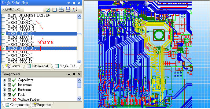
2.2 DQ0~DQ7、DQML、DQSL_P、DQSL_N
2.3 DQ8~DQ15、DQMH、DQSH_P、DQSH_N
-
3.1 A0~15、BA0、BA1、BA2、ODT、/CS、/WE、/RAS、/CAS、/RESET、CLK
-
Questions and Discussions
5.1 How to create the ports of DDR group automatically in SIwave?
5.3 How to use DDR IBIS model with ODT enable in Designer?
5.4 How to calculate DDR bit time for unit interval of eye in Designer?
5.5 How to show different lines with different color in Designer v6.0?
5.6 How to set "eye measurement" in Designer v6.0?
5.7 How to edit a single-end IBIS IO to be a differential IO?
5.8 How to set DQS phase on the center of DQ eye?
5.9 Why to use different "seed" setting in V_PRBS properties?
5.10 What is the effect of input signal tr, tf?
5.11 There is no any series resistor (Rs) on data or address lines, why?
5.12 The serpentine layout is necessary for "this" DDR3 design or not?
![]()
1.1 Double Data Rate SDRAM
1.2 Different Group Strobe by Different CLK Signal
1.3 DDR、DDR2、DDR3、LPDDR (Low Power DDR)=MDDR (Mobile DDR)
2.1 Ansoft SIwave and Designer Setting
2.1.1 Add ports and export 20 ports touchstone file (.s20p) from SIwave
Don't use "#" as a net name or port name, otherwise it will be something wrong to touchstone file (.snp)
2.1.2 Download Micron DDR3 IBIS
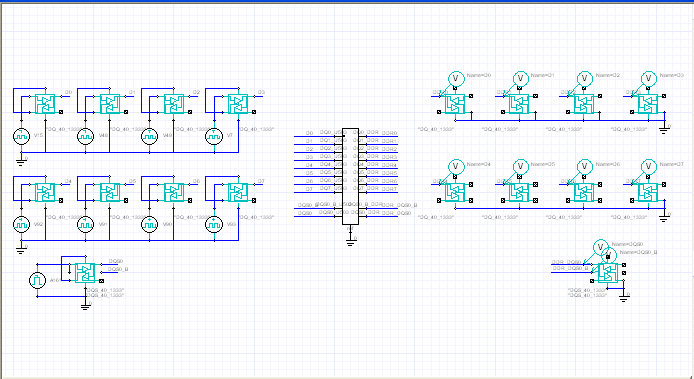
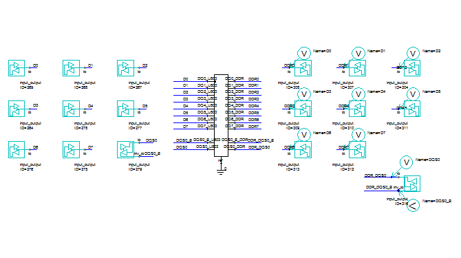
2.1.3 Add pattern source (V_PRBS)、Nport model、IO IBIS model and connect all the nets automatically by Designer
2.2 DQ0~DQ7、DQML、DQSL_P、DQSL_N (means low byte data group, and differential strobe clock)
2.3 DQ8~DQ15、DQMH、DQSH_P、DQSH_N (means high byte data group, and differential strobe clock)
3.1 A0~15、BA0、BA1、BA2、ODT、/CS、/WE、/RAS、/CAS、/RESET、CLK
4.1 Unify the method to import IBIS and IBIS-AMI:Tools \ Import IBIS Components
4.2 Simplify the IO symbol for IBIS and IBIS-AMI
4.3 Merge all IO settings (input/output buffer, power connect, input pattern source define...) in the properties of symbol internally
You can see the circuit in 2.1.3 become very simplified and easy as next
-
Questions and Discussions
5.1 How to create the ports of DDR group automatically in SIwave?
Select all the nets which to be added ports, and Circuit Elements \ Generate on Selected Nets
refer to 延伸閱讀02, step65.2 How to connect the nets from pattern source (V_PRBS) to a circuit symbol (.s20p) automatically in Designer?
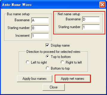
Select all the nets which to add port first, and Schematic \ Auto-Name Wires
5.3 How to use DDR IBIS model with ODT enable in Designer?
5.3.1 There are different methods to implement ODT effect by IBIS, for example, Micron uses [add submodel] grammar. Refer to Designer\Lesson 5 step 3.1.4 or Designer\Lesson 7 step 3.5, and select IO "model" in [parameter value tab].
5.3.2 Other chip venders (like Intel), may provide stand along IBIS model for ODT, or a [Terminator] behavior model. Refer to Intel IBIS and check the difference between dq_5_29_diff.ibs and dqodt_100_diff.ibs
5.3.3 If use Samsung IBIS, and import DQ_PIN (6 port I/O symbol) first, and run it well, then directly change the model to DQ_ODT_60(4 port input symbol), simulation will be wrong. why?
The type of Designer symbol have to match IBIS model type, so 6 port symbol is wrong for DQ_ODT_60 model type.
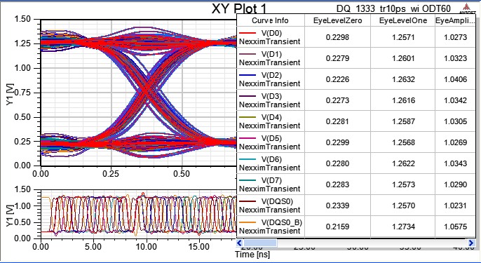
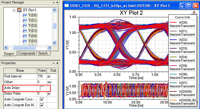
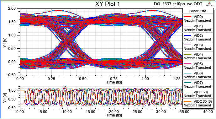
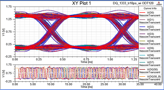
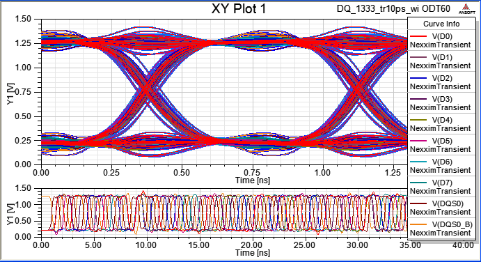
5.4 How to calculate DDR bit time for unit interval of eye in Designer?
DDR3-1333 for example:
1/1333MHz=750ps with rising time=falling time about 200ps
CLK diff. period = DQS diff. period = 750ps*2 = 1.5ns,
By the way, refer to DDR3_Standard_Specification_JESD79-3B
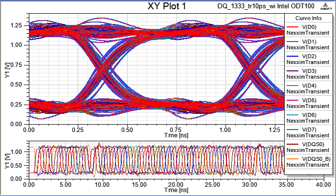
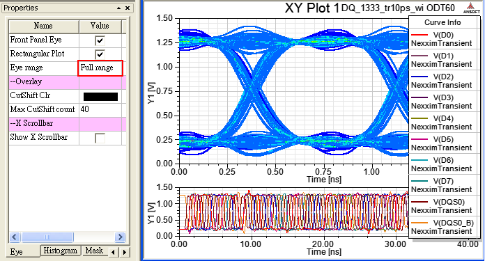
5.5 How to show different lines with different color in Designer?
5.5.1 Left-click the eye plot window, and check the [Properties window] as below
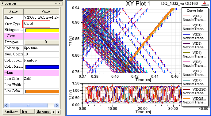
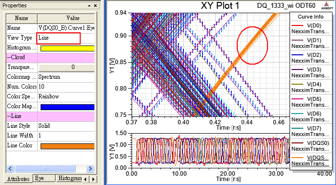
5.5.2 Zoom in eye waveform, and left-click DQS0_B for example to check [View Type] in the Properties window
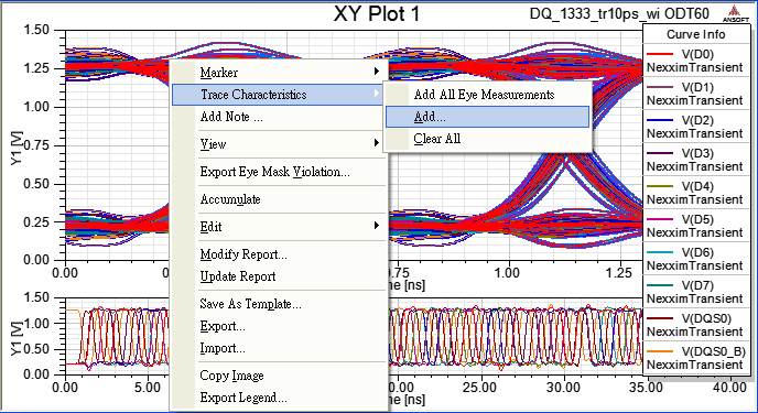
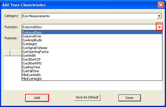
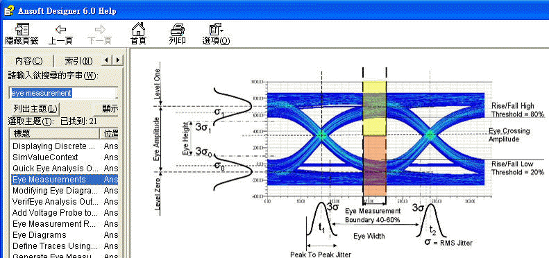
5.6 How to set "eye measurement" in Designer v6.0?
right-click and select [Trace Characteristics] \ [Add] or [Add All Eye Measurements]
Select which items to measure
if select [Trace Characteristics] \ [Add All Eye Measurements]
By the way, you can use help to see the [eye measurement] function define
5.7 How to edit a single-end IBIS IO to be a differential IO?
Please refer to Designer \ AN 004:Eye Analysis for Differential pair part II
5.8 How to set DQS phase on the center of DQ eye?
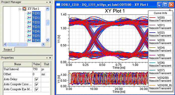
5.8.1 set TD (delay time) of DQS source (V_CLOCK_W_JITTER) is half period, means 375ps.
5.8.2 select all nets, and disable [Auto Delay] function
5.9 Why to use different "seed" setting in V_PRBS properties?
To involve Intersymbol Interference(ISI) and crosstalk induced jitter.
5.10 What is the effect of input signal tr, tf?
Please refer to Designer \ AN 004:Eye Analysis for Differential pair part II, and
-- Set V2 = 1V, tr=tf=200ps, PW=550ps, the simulation:the cross point level is on central
-- Set V2 = 1.5V, tr=tf=200ps, PW=550ps, the simulation:the cross point level is on central
-- Set V2 = 1.5V, tr=tf=100ps, PW=650ps, the simulation:the cross point level is on central
5.11 There is no any series resistor (Rs) on data or address lines, why?
Because the project is a notebook mother board, and it uses DDR3 DIMM with external Vtt terminator.
Please refer to Designer \ Lesson 7:DDR and ODT simulation.5.12 The serpentine layout is necessary for "this" DDR3 design or not?
It will be decided by co-simulation with DIMM module.
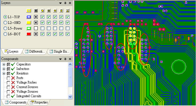
5.13 Is there any DDR3 layout notice in the PCB?
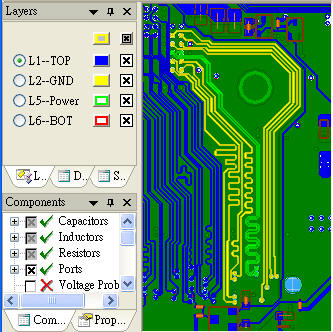
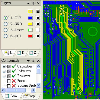
5.13.1 The lines which belong to the same group, will be routed on the same layer
5.13.2 All the anti-pad voids of DDR3 (just under BGA), keep the return path continuous on reference plane.