線上影音
Home > ANSYS HFSS 教學 > HFSS vs Q3D for Rdc, and Layered Impedance for Cu-Ni-Au Coating
HFSS是學界、業界電磁模擬軟體的標準,過去唯二美中不足的地方是:模擬時間較長、DC求解不夠準。HFSS v15 (R14.5, 2013)具體改進了這兩個問題:前者以全新的HPC分散式處理技術,隨著硬體CPU核心數的增加,接近線性的縮短模擬時間,後者則是以surface impedance boundary condition(SIBC)技術,大幅提升HFSS解傳輸線DC的模擬準度。
本文始於2012年,並於2018年修訂,新增鍍層金屬結構(Cu-Ni-Au)寬頻解析的探討。主要驗證HFSS的DC準度(以Q3D交叉比對),並介紹表面邊界技術(SIBC)與內部解析(solver inside)技術。R19.2的DC與低頻準度又更好。
This article started in 2012, and was revised in 2018 to add the discussion about Cu-Ni-Au coating structure. It is intended to verify the DC accuracy of HFSS, and introduce the surface impedance boundary condition (SIBC) and solver inside technology in HFSS. R19.2 HFSS enhances DC and low frequency interpolating further.
-
Microstrip Line
-
2 layer DDR Design
-
Cu-Ni-Au Coating Structure
3.1 Transmission Line (w>>h) one surface coating with HFSS R19.3
3.2 Transmission Line (w=h) one surface coating with HFSS R19.3
3.3 Transmission Line (w=h) four surfaces coating with HFSS R19.3
-
Q&A 問題與討論
5.1 How to convert R from SYZ of HFSS?
5.2 Why are Re(1/Y11) and Re(Z11) different? (important)
5.3 When may you need to select "solve inside"? (important)
5.4 Is there any special intrinsic character for a Ni coating?
5.5 How to assign [DC Thickness] of solid materials in HFSS?
5.6 When is it necessary to set [Advanced DC Extrapolation]?
5.7 What is the difference to assign "Effective" or "Manual" DC thickness?
5.8 What is the difference between [Assign DC thickness], [Finite conductivity] and [Layered Impedance]? (important)
![]()
-
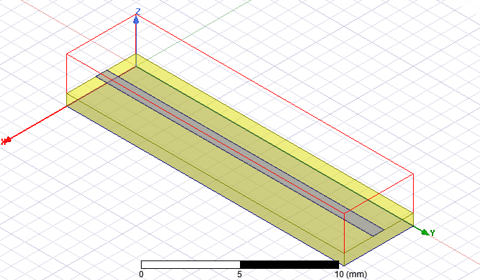
Microstrip Line
1.1 20mm microstrip line with HFSS R19.2
1.1.1 Real copper thickness w/i "solve inside"
走線為具實體厚度0.7 mils的copper,並對其設定solve inside。It takes more time, and R will be mesh-sensitivity.
1.1.2 Real copper thickness w/o "solve inside", and assign effective DC Thickness boundary by default (推薦最佳做法)
走線為具實體厚度0.7 mils的copper,默認設定no solve inside,並且assign effective DC Thickness boundary by default.
It is the official suggestion to get more accurate RDC with HFSS for SI application.
使用[Assign DC Thickness]必須滿足兩個條件:不能設solve inside,且是夠薄的導體.
1.1.3 Assign [finite conductivity] boundary on sheet with one-sited surface impedance boundary condition (SIBC)
走線不具實體厚度,以assign [finite conductivity] boundary設定成厚度0.7 mils的copper.
1.1.4 Real copper thickness w/o "solve inside", assigning [finite conductivity] boundary for roughness usage
走線為具實體厚度0.7 mils的copper,默認設定no solve inside,但多放了[finite conductivity]在走線上,為了設roughness之用
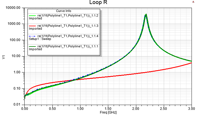
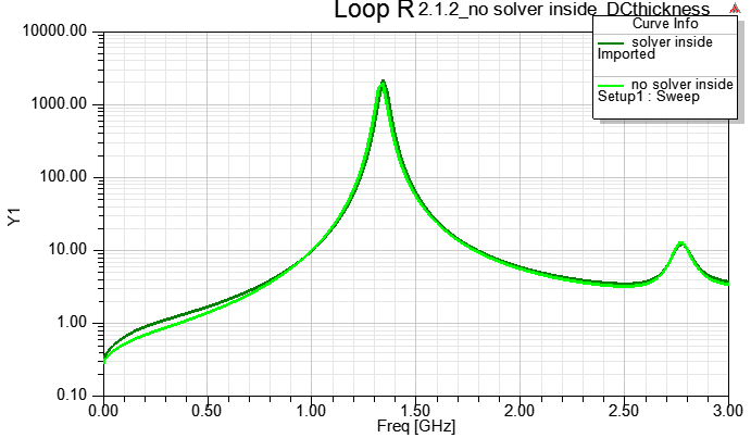
從以上實驗結果可知,對於傳輸線,不論有沒有設定solver inside,HFSS都可以得到準確的DC R=0.024 ohm。但記得不要以厚度0的sheet來當走線。
1.2 20mm microstrip line with Q3D R19.2
由於Q3D是靜磁場求解,有1/10波長頻寬限制,對此例20mm長的傳輸線來說,大約只適合解到0.75G,頻率再上去就會遇到一階共振點把阻抗抬升,而這效應(共振)所增加的R只有HFSS有考慮。
即使觀察0.75G以內,HFSS與Q3D的AC R還是有些不同,這差異的主因是:此例的GND plane sheet,在HFSS內是 用PEC boundary,在Q3D內是0.1mm的thin conductor boundary,前者的阻抗還是比較小。
Q3D只能考慮肌膚效應所造成的R隨頻率增加而上升的效應,HFSS除了能考慮肌膚效應還能考慮因共振所造成的R增加。
-
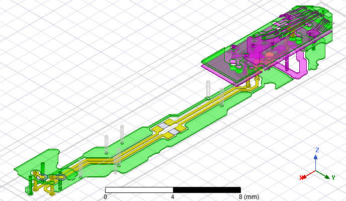
2 layer DDR Design
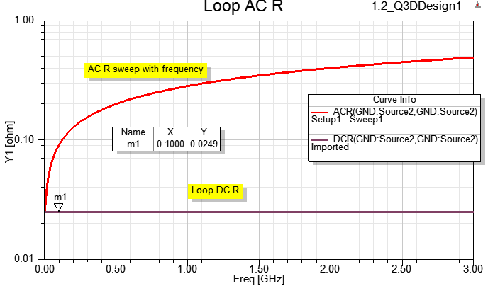
2.1 2 layer DDR design with HFSS R19.2
Real copper thickness w/o "solve inside" assigning [DC Thickness] vs. w/i "solver inside"
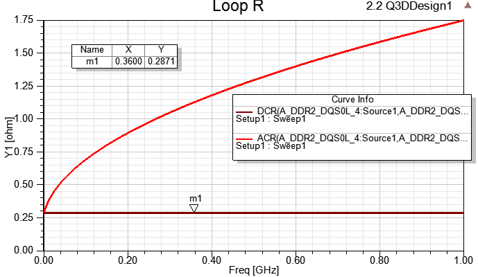
2.2 2 layer DDR design with Q3D R19.2
-
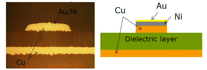
Cu-Ni-Au Coating Structure
對於金屬鍍層(如銅鎳金),HFSS內最佳實踐方式是[Layered Impedance] boundary。
[Layered Impedance]不只可以是導體(金屬)材料,也可以是介質。HELP內有特別說明
當[Layered Impedance]設置在某個no solver inside的3D導體表面時,該導體原本在[Assign DC thickness]內的屬性會改以[Layered Impedance]屬性取代,所以在[Layered Impedance]內的layers list必須包含最底(基)層的金屬。
The first layer in the layers list is the top layer, the order is important, if it is reversed, the R result will different as well. 上層方向指的是肌膚效應電流聚集方向
HFSS默認解導體的[Assign DC thickness]技術,其估算厚度=2*體積/表面積,請參考5.7。
而[Layered Impedance]最底層金屬厚度估算則分兩種情況:
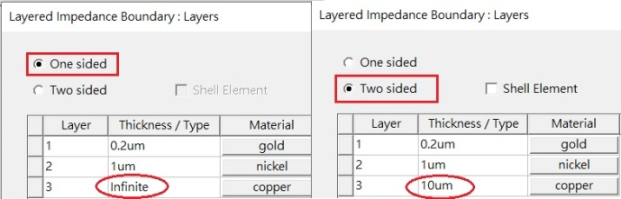
-- 對於[Layered Impedance]設在3D金屬物件的表面,即所謂的one side,最底層厚度直接設"infinite"
.. (但對於一個"四面"都設layered impedance的銅條,如探針模擬,有另外設定方式)
-- 對於[Layered Impedance]設於2D物件,即所謂的two side,最底層厚度直接設導體厚度
若銅導體四個面都鍍層,又透過實體厚度建模,即鎳金外層相當於是包覆整個銅導體的空殼。這時鎳金薄殼不能以[Assign DC thickness]求解,否則會導致設置的HFSS port只看到最外層的金表層,看不到內部的銅與鎳。也就是[Assign DC thickness]無法處理"大腸包小腸"式的包覆/封閉式鍍膜結構,DCR會暴增(as 3.3.3)。
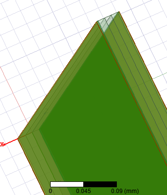
3.1 Transmission Line (w>>h) one surface coating with HFSS R19.3
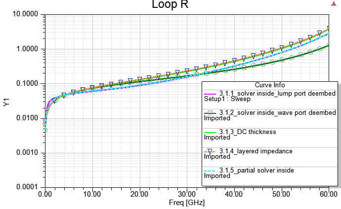
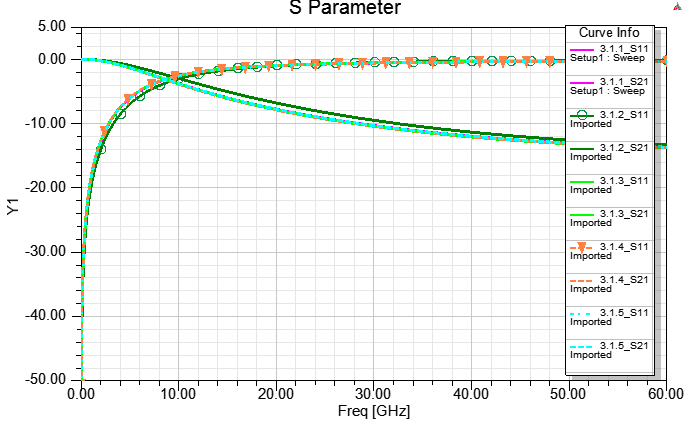
3.1.1 Real Cu/Ni/Au thickness "solve inside" with mesh option/seed, and lump port de-embedded (DC最準)
3.1.2 Real Cu/Ni/Au thickness "solve inside" with wave port de-embedded (DC最準, 高頻準度也ok)
3.1.3 Real Cu/Ni/Au thickness "no solve inside", and assign "effective" DC thickness
3.1.4 Real Cu thickness, and set [layered Impedance] on a coating surface of the copper object (一般的默認作法)
3.1.5 Real Cu/Ni/Au thickness, "solve inside" for Ni/Au, and "no solve inside" for Cu (partial solver inside)
3.1.4例中,是把[Layered Impedance]放在銅表面,然後再於layers list內分別定義銅鎳金厚度與堆疊次序。我們也可以把[Layered Impedance]放在金表面,然後再於layers list內分別定義銅鎳金厚度與堆疊次序。兩者的結果會非常接近,而後者會更貼近3.1.2。
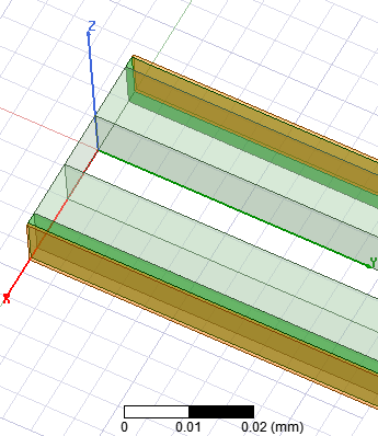
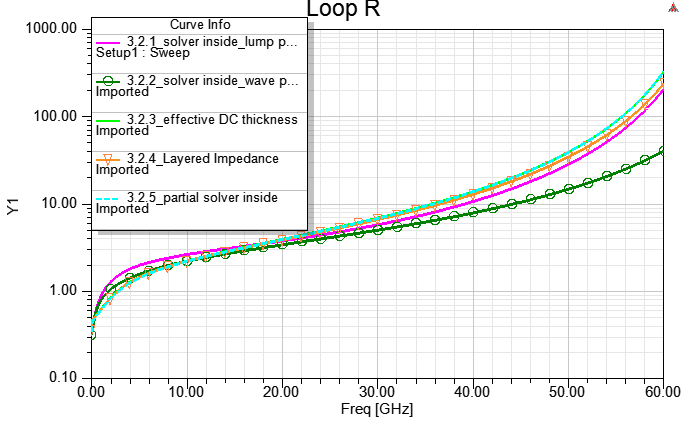
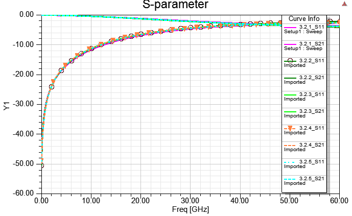
3.2 Transmission Line (w=h) one surface coating with HFSS R19.3
3.2.1 Real Cu/Ni/Au thickness "solve inside" with lump port de-embedded (DC最準)
3.2.2Real Cu/Ni/Au thickness "solve inside" with wave port de-embedded (DC最準, 高頻準度也ok)
3.2.3 Real Cu/Ni/Au thickness "no solve inside", and assign "effective" DC thickness
3.2.4 Real Cu thickness, and set [layered Impedance] on a coating surface of the copper object (一般的默認作法)
3.2.5 Real Cu/Ni/Au thickness, "solve inside" for Ni/Au, and "no solve inside" for Cu (partial solver inside)
許多人誤以為solver inside除了求解時間較長,是沒有其他副作用的最準解法。對於任意結構 的"DC準度",Solver inside確實是最靠譜的做法,但當導體進入高度肌膚效應區時,由於FEM很難在導體表面有足夠多/好的網格分佈,導致solver inside對較厚/大的導體在"高頻"的求解準度不足。 一般建議 :如果要使用solver inside,導體厚度不要超過5倍的肌膚深度。Solver inside makes Rdc accurate, BUT Rac NOT guarantee while copper thickness is larger than 5*skin-deep, due to mesh performance (mesh-sensitivity).
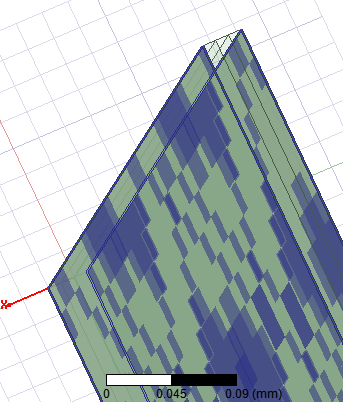
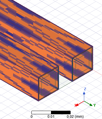
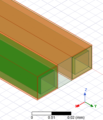
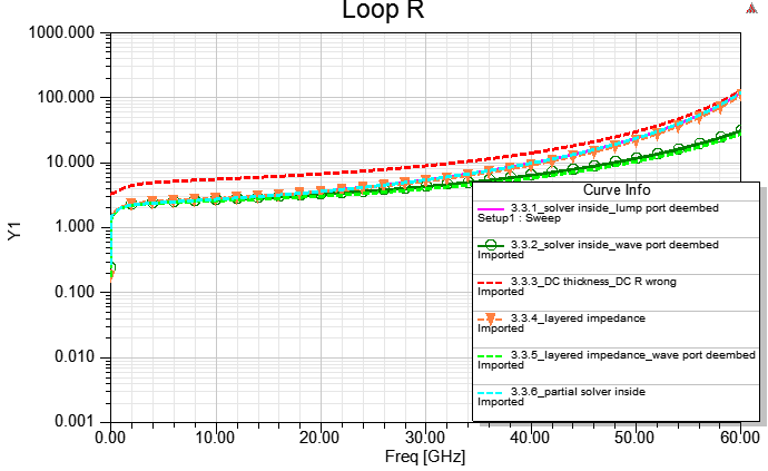
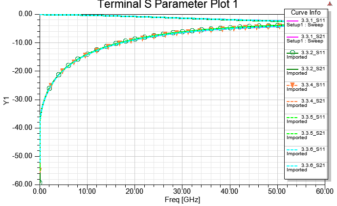
3.3 Transmission Line (w=h) four surfaces coating with HFSS R19.3
3.3.1 Real Cu/Ni/Au thickness "solve inside" with lump port de-embedded (DC最準)
3.3.2Real Cu/Ni/Au thickness "solve inside" with wave port de-embedded (DC最準, 高頻也ok)
3.3.3 Real Cu/Ni/Au thickness "no solve inside", and assign "effective" DC thickness (DC R wrong, much larger)
3.3.4 Real Cu thickness, and set [layered Impedance] on four coating surfaces of the Cu object (推薦)
3.3.5 Real Au thickness, and set [layered Impedance] on four coating surfaces of the Au object with wave port de-embedded (推薦)
3.3.6 Real Cu/Ni/Au thickness, "solve inside" for Ni/Au, and "no solve inside" for Cu (partial solver inside)
3.3.4/3.3.5特別值得一提的地方:把[Layered Impedance]設在金的表面,鎳銅層是透過layers list內的設定來實現。這樣建模的好處是,與3.3.1/3.3.2相比,線間距條件才是真的完全一致,這樣做結果比對會更正確。所以,使用[Layered Impedance]解銅鎳金鍍層的題目,可以把BC設在銅表面往外看(3.1.4/3.2.4),也可把BC設在金表面往內看(3.3.4/3.3.5)。兩種設法 結果差異其實很小,但後者因為有考慮鎳金厚度所貢獻的空間距離,較貼近實際物理條件。
[Layered impedance] is used for coating application
Two-sided shell element is used for shielding effect analysis (S.E.)
[Finite conductivity] is used for setting roughness on a metal surface
如果要使用solver inside,一般建議"導體厚度不要超過5倍的肌膚深度"。
對於SI的模擬應用,訊號線部分不好用0厚度sheet建模,不管是用one-sided或two-sided shell element。
SIBC的主要觀念是:高頻肌膚效應區透過boundary(SIBC)解,低頻區透過DC thickness估算出,所以如何估出等效DC thickness很重要
HFSS默認解導體的[Assign DC thickness]技術,其估算厚度公式請參考5.7。[Layered Impedance]的厚度估算則沒有公式。
HFSS轉出來的是loop RL,Q3D解出來的是partial RLC,兩者物理意義不同。若要拿Q3D的結果與HFSS比對,除了要注意1/10波長頻寬限制,還必須在Q3D內使用return path以得到loop
-
Q&A 問題與討論
5.1 How to convert R from SYZ of HFSS?
Ans:R = Re(1/Y11),Y11倒數取實部
5.2 Why are Re(1/Y11) and Re(Z11) different?
Ans:As we know, Z=R+jwL, Y=G+jwC, and Y=1/Z. But Re(1/Y11)¹Re(Z11), why?
Because Y matrix gives the input admittance value when all the other terminals are short.
5.3 When may you need to select "solve inside"?
Ans:
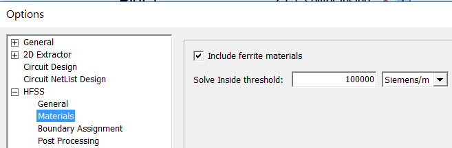
In HFSS, objects with material's bulk conductivity > 105sem/m (as copper) will not be checked "solve inside" by default, and this threshold can be set from [Tools] \ [Options] \ [General Options].
To consider the current distribution inside a conductor, Shielding Effectiveness/Isolation analysis, or conductor thickness is thinner than skin depth (in general, poor conductor or very low frequency), you may need to check "solve inside".
以下是幾種可能會使用solver inside的時機:
Verify DC accuracy of SIBC
Die-level component extraction, as inductor
S.E. analysis of a real thickness shielding ca
5.4 Is there any special intrinsic character for a Ni coating?
Ans:鎳塗層本身是沒有需要特別討論的地方,但Cu-Ni-Au製程倒是有一個特殊性值得跟大家介紹。
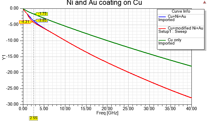
Cu-Ni-Au這種製程,量測微帶線入射損耗會發現在2~3GHz會有輕微下凹的現象[1], 這現象目前除了學術性論文上有討論,並沒有見到任何商用電磁模擬軟體可以做出這效應。原因我們接著說明...
各位可以參考[2]說明這現象背後的"可能"物理成因:(假設)是Ni夾在Au與Cu間, 能量在磁性材料間共振造成的。也就是說,這現象不是coating Ni就會發生,而是要coating兩層材料,把導磁性材料夾中間才會發生。這最早於1935年的paper提出,需要對Ni材料提出一種特殊的model (with 5 parameters),來fitting這下凹的結果。這現象不是單單材料導電性,與導磁性能描述的。
Even taking the process variation into account, there is still an anomalous behavior in the losses and propagation delay of microstrips with nickel plating which cannot be explained using a simple value of permeability or resistivity for the nickel.
However, by applying a model, first introduce by Landau and Lifshits in 1935, they are able to match the measured performance pretty well. This assumes a resonance in the magnetization between layers in the nickel plating. This model for the nickel properties has just five parameters that fully describe it.
HFSS模擬這Cu-Ni-Au coating的方法是用Layered Impedance BC,可以很正確的做出入射損失,但不含這低頻共振下凹的現象。如果硬是要搞一個在低頻loss變差的結果,就是給鎳指定一個隨頻率變化的導電率與導磁率。這方法 雖然可以得到passivity與causality的下凹S21,但無法得到預期的group delay,免強只能說是個workaround。
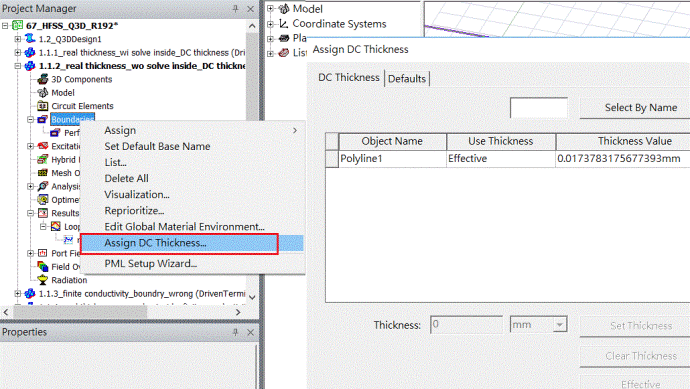
5.5 How to assign [DC Thickness] of solid materials in HFSS?
Ans:There are two ways to assign DC Thickness:[HFSS] \ [Boundaries] \ [Assign DC Thickness] or right-click as below
注意,在surface上right-click選[Assign Boundary]是沒有[Assign DC Thickness]項的
5.6 When is it necessary to set [Advanced DC Extrapolation]?
Ans:
從本文以上介紹可以理解,要讓HFSS解DC較準的方法,是使用DC thickness BC技術,而不是用[Advanced DC Extrapolation],後者也是常被誤用的壞習慣。 [Advanced DC Extrapolation]只用於少數特殊情況,建議默認使用[Standard DC Extrapolation],因為前者可能造成non-passivity問題 。
比方說:對於不適合用SIwave解的SI+PI co-sim題目(如兩層板PCB設計),當我們用HFSS求解時,如果在VDD-GND上有很大的去耦電容(lump C 10u~100uF),會導致該路電源的S參數在低頻有劇烈變化,這時使用[Advanced DC Extrapolation],指定最低求解頻率數十Hz會有幫助。但即使是這種情況,使用[Advanced DC Extrapolation]也不是最好的作法,因為可能無法滿足passivity/causality。最好的做法是HFSS抽模型時不含這電容,在大電容接點留port於circuit level外加該大電容,或是採用2021R2以後新版HFSS提供的[Enhanced low frequency accuracy] option.
5.7 What is the difference to assign "Effective" or "Manual" DC thickness?
Ans:
"Effective"是以DC thickness@2*volume/surface area來計算DC thickness,這對於薄的導體結構是很準的,但對於圓柱形的結構(如bond wire),此時就可以用"Manual"把等效的導體厚度設成圓的半徑即可。(請參閱HFSS HELP說明, look for key word "calculating finite thickness impedance")
-- 很薄的導體,使用effective DC thickness (default setting),或導體厚度當thickness
-- 圓柱形導體,且長度遠大於半徑,使用effective DC thickness =半徑 當DC thickness
-- 正方形銅柱,且長度遠大於邊長,使用effective DC thickness = 0.5*邊長 當DC thickness
5.8 What is the difference between [Assign DC thickness], [Finite conductivity boundary] and [Layered Impedance]?
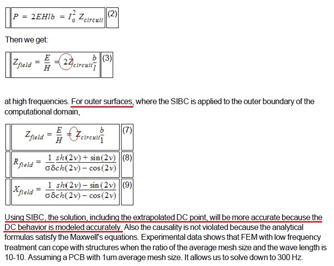
Ans:After searching HFSS HELP for the key words "DC thickness", "Finite conductivity boundary", "Layered impedance" and "SIBC", you can find similar UI settings for SIBC from [Finite conductivity] and [Layered impedance] boundary, but not [Assign DC Thickness].
From above figure, we note there are two types of formulas for SIBC, one is internal boundary as (3), the other is outer boundary as (7).
Both of [Assign DC thickness] and [Finite conductivity] use the SIBC technology to calculate, but the formulas are not exactly the same. [Assign DC thickness] uses internal boundary only, but [Finite conductivity boundary] and [Layered impedance] use internal or outer boundary by user definition.
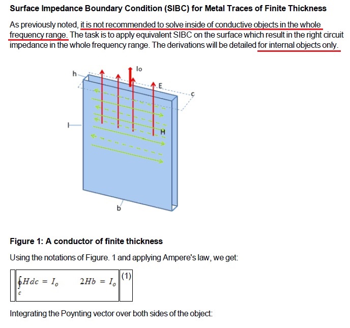
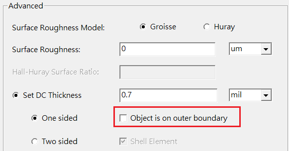
[Finite conductivity boundary] uses [one-sided] with [Object is on outer boundary] unchecked by default, and it means the condition of internal boundary. While in old HFSS R14.5 version, [Finite conductivity boundary] only supports outer boundary, to be consistent to such condition, please check [one-sided] and [Object is on outer boundary] both.
- 過去舊版的HFSS R14~R15,由於[Assign DC thickness]是internal boundary, 而[Finite conductivity]僅支持outer boundary,如果在3D導體的表面放[Finite conductivity]等於是把outer boundary套用於internal boundary, 所以[Finite conductivity]內所設的導體厚度要再除二,DC R值才會對。R15(2016)以後的新版只需要[Finite conductivity]設定one-sided with "Object is on outer boundary" uncheck, 不再需要把DC thickness除二,DC R答案就是對的(如Surface roughness 5.1.3所示)。
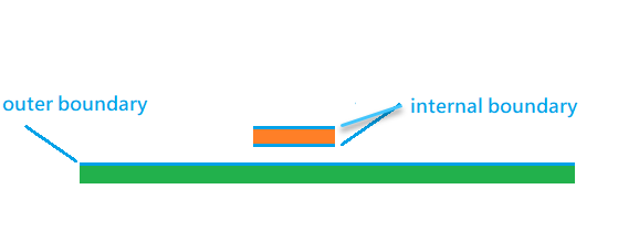
One-sided : 使用於3D導體的表面
- 若導體貼background (outer boundary),或本身是良好的參考平面,則勾選"object is on outer boundary"。
對參考平面來說,勾不勾"object is on outer boundary"一般差異很小。- 若要用於走線(signal),因上下兩側都有H,所以計算出來的阻抗Z會是outer boundary的兩倍,如上上圖內(3)式所示,此時就不勾選"object is on outer boundary"。(此時也就是採用two-side的BC技術)
對走線來說,勾不勾"object is on outer boundary"差異就很明顯,但只在低頻(0~200MHz)有影響。Two-sided:使用於零厚度的sheet for S.E. (若有勾選shell element可進一步提高高頻準度)
[1] Yuriy Shlepnev, "Nickel Characterization for Interconnect Analysis", IEEE Int. Electromagnetic Compatibility (EMC), 2011.
[2] Impact From Electroless Nickel on Microstrip Insertion Loss and Propagation Delay