Online video
Home > ANSYS HFSS 教學 > Surface Roughness Effect
This article started in 2014 and was revised in the middle of 2015 ans 2020. It is intended to introduce the surface roughness effect and different roughness models with ANSYS R16 SIwave and HFSS. "Surface roughness" is a very hot topic recently, and there are six papers to talk about this on DesignCon 2014 and DesignCon 2015.
-
Hammerstad Model
-
Huray Model
3.2 Misunderstanding for Current Flow and Power Loss in Hammerstad Model
-
Roughness model in HFSS
-
Q&A
8.2 Does roughness affect DC R?
8.3 Which roughness model is better?
8.4 How to simulate the resonance absorption valley at 35GHz in step 3.3?
8.5 Does SIwave consider surface roughness with "top/bottom" or "top/bottom and side" surface?
8.6 The Hammerstad used in ANSYS EBU is classic or modified Hammerstad model?
![]()
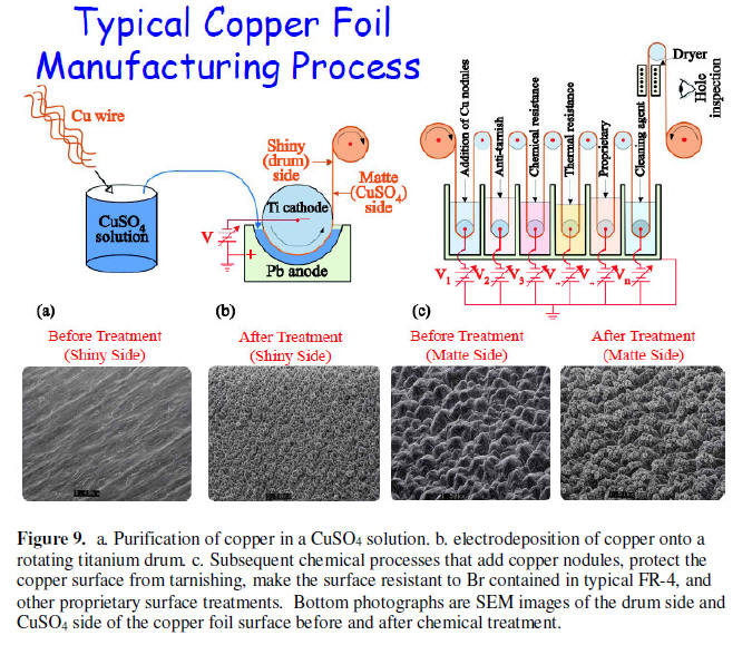
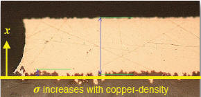
The surface roughness comes from the material processing procedure [1]p.11, and its purpose is to increase the adhesion between the copper foil and the glass fiber (FR4).
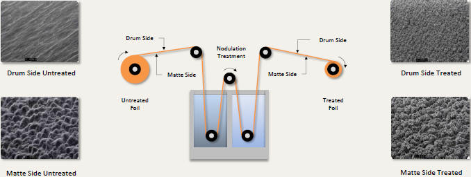
The copper foil will have a flat side (drum side) and a rough side (matte side). [11]p.22
To allow the copper foil to be thermally bonded to the dielectric material (FR4, glass fiber woven), the interface between the copper and FR4 is usually rough. [1]p.10,12
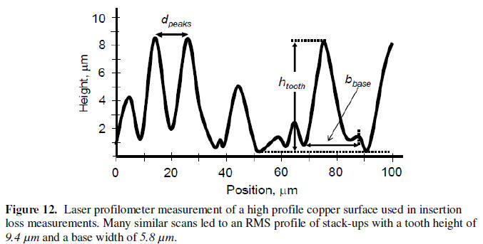
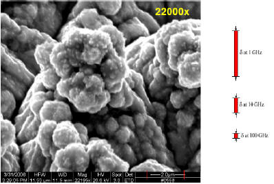
Laser profilometer can get the RMS profile of copper surface. [1]p.13
The height of tooth height is typically 0.3-5.8um in RMS value and the peak with 11um. [2]p.38
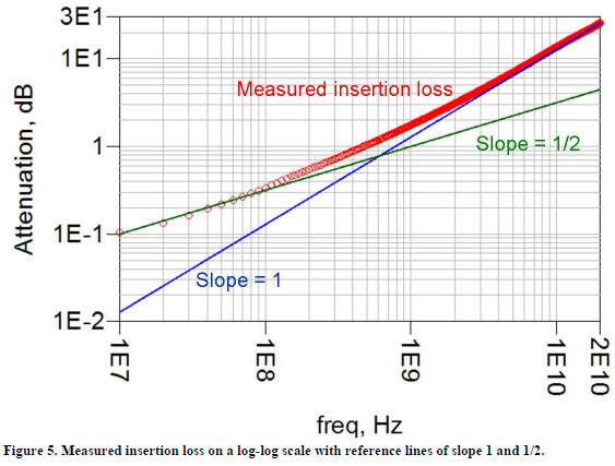
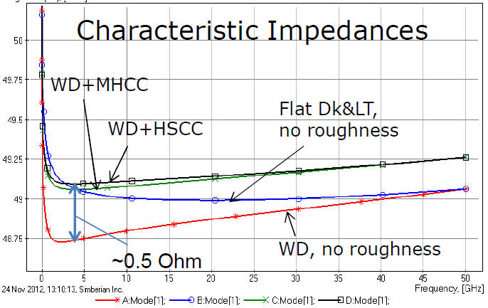
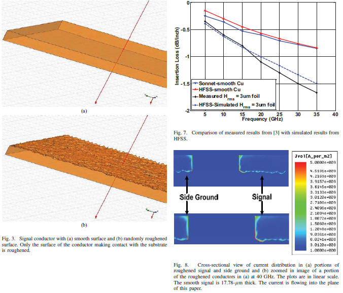
The surface roughness has little effect on the characteristic impedance (about 0.5ohm), but it has a great effect on the insertion loss at high frequencies (maybe more than 30%). [3]p.15
The insertion loss is mainly affected by conductor loss at lower frequencies (mainly skin effect), and by dielectric loss at higher frequencies. [3].p3-4
Total lose = LossC (conductor loss) + LossD (dielectric loss), LossDµFrequency, [4]p.7,11
Conductor loss = LossK (skin effect loss) + LossS (scattering loss), LossKµSquare root of Frequency
To select the appropriate roughness model with a defined cross-section. [3]p.16
-
Hammerstad Model
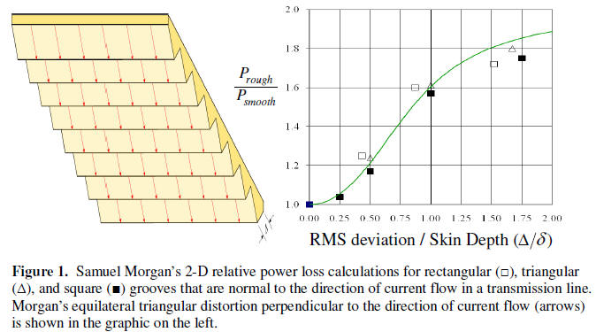
2.1 Hammerstad Model (1980)
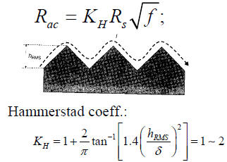
The definition of the Hammerstad Model is as follows: impedance increases with frequency when high-frequency signals flow, and skin effect and surface roughness need to be considered at the same time. Under the condition that the skin effect is established, Rac is proportional to the root of the frequency, plus a Hammerstad coefficient (KH) responsible for introducing the influence of surface roughness, forming the following mathematical formula: [2]p.41
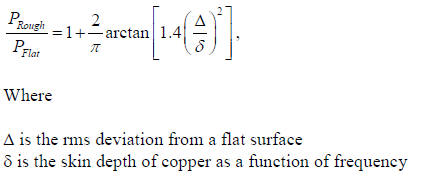
Another physical meaning of this KH coefficient is Prough/Pflat [1]p.3
The Hammerstad model breaks down in case of a very rough copper foil, so other models are needed.
The Hammerstad model saturates at 2, not enough loss for rough copper. It is usually used ONLY FOR HRMS< 2um. [2]p.46
Hammerstad Model is based on the Morgan model (1949), which assumes that the current flows along the jagged surface of the rough surface (only described by the 2D quasi-static form of Maxwell equation), and the loss is related to D/d. Please note that the behavior is just Morgan's assumptions without any theoretical basis. By the way, because the KH value is only between 1 and 2, and it will saturate when KH is over 2, it is only suitable for low roughness model (average size RMS=1um. [1]p .12, [3]p.10).
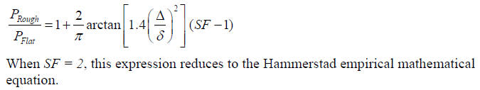
2.2 Modified Hammerstad Model (2013), [3]p.10
The SF item (or RF item) is added here, to make Hammerstad Model not saturated for roughness when HRMS>2um.
D=HRMS, and SF means Scaling Facto.
The physical meaning of SF factor, as the roughness factor (RF) showed below:
Hammerstad Model just needs the parameter Delta (D=HRMS) for roughness definition, that is, Rq and Rq@Ra. [5]p.13,15,16
-
Huray Model (2009)
3.1 What is Huray model
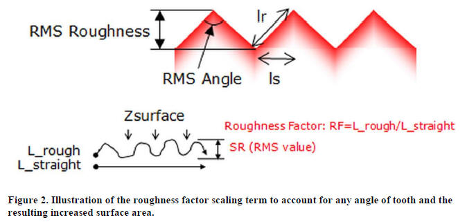
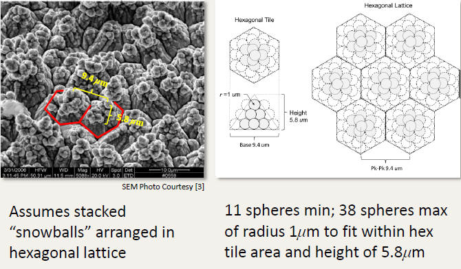
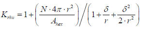
Although the aforementioned Hammerstad and modify Hammerstad model require the tooth texture profile RMS parameter (D) only, they do not have a theoretical basis. In the real physical structure, the shape of the particles on the metal surface is as below, described by 3D snowball model.
Assume the bottom area unit is formed by a hexagon, and each unit is piled into a pyramid shape with a different number of spheres. [11]p.31
[3]p.10
[1]p.21, [3]p.9
Even though I have tried to explain it, for most people, you may be still unclear...especially how to understand the physical meaning of a bunch of symbols in the above formula?
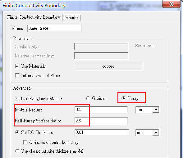
In fact, the spirit of Huray model is to describe any degree of the roughness by a defined snowball size(ai) and snowdrift size(Ni/Aflat). When you implement Huray model in SIwave and HFSS, the two parameters you have to input are"Nodule Radius" and "Huray Surface Ratio (SR)", that exactly imply the snowball size and snowdrift size.
That is why in SIwave GUI, by default, a fixed nodule radius value (0.5um) is proposed for the three levels of roughness setting with the different SR=1/3/6. Such way can be usderstood through a physical meaning -- the nodule radius is the minimum element size of the snowball model, and it generally does not vary with roughness degree [1]p.12, therefore to fix nodule radius and adapt SR not only can get the loss effect of any degree roughness but also make sense in physical.
How to use Huray model? How to input these parameters of Huray model? Please refer to 8.7
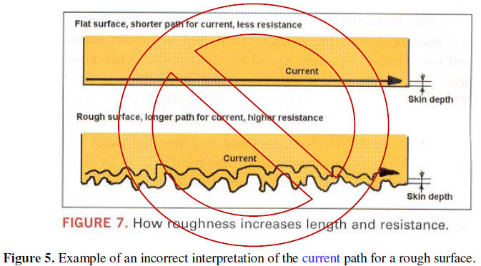
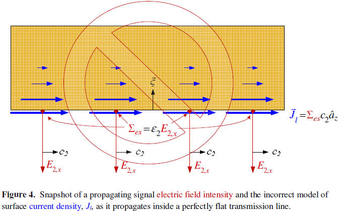
3.2 Misunderstanding for Current Flow and Power Loss in Hammerstad Model [1]p.5~9
Morgan model assumes the current flowing along on the conductor rough surface as 2.2 shows. It is not correct.
If the assumption Hammerstad proposed is correct, why the propagation delay does not increase with roughness?
The answer is that local surface charge density is formed by the displacement of conduction electrons transverse to the surface profile so that a wave of charge density propagates at whatever speed is needed to support the external electric field intensity in the transmission line. No charged particles actually move at relativistic speeds so we need not take into account space contraction.
When current flows in a conductor, assuming that the current distribution decays exponentially with the depth of the conductor, the model is not correct either.
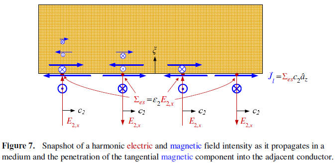
The correct description should be understood through the concept of field propagation, as shown below (eddy current).
The blue solid (with arrow) line represents the current (direction), the blue circle represents the entry and exit of the magnetic field, and the red solid (with arrow) line represents the electric field (direction).
Because the propagation speed of electric field in the medium is C2=C/√4=C/2, the propagation speed of charge density on the surface of adjacent conductors is also C2=C/2.
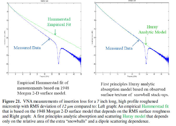
3.3 Measurement v.s. Simulation
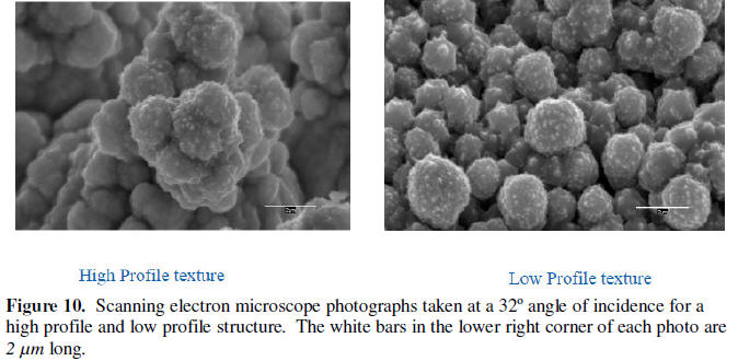
Huray model is good for high profile roughness. [1]p.21
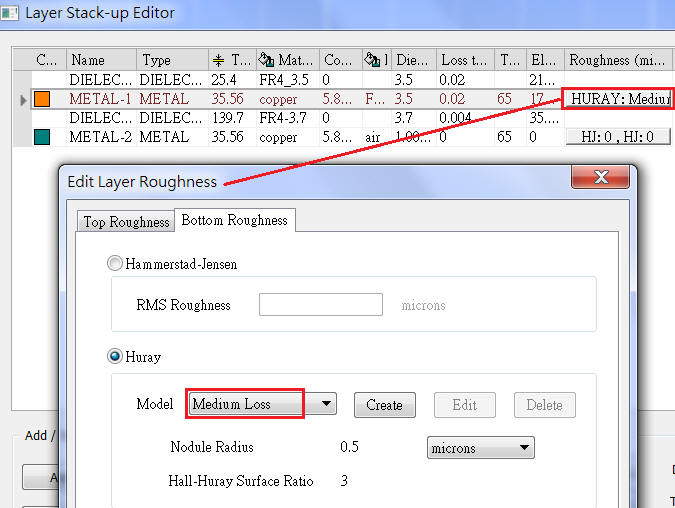
4.1 [Edit] \ [Layer Stack]
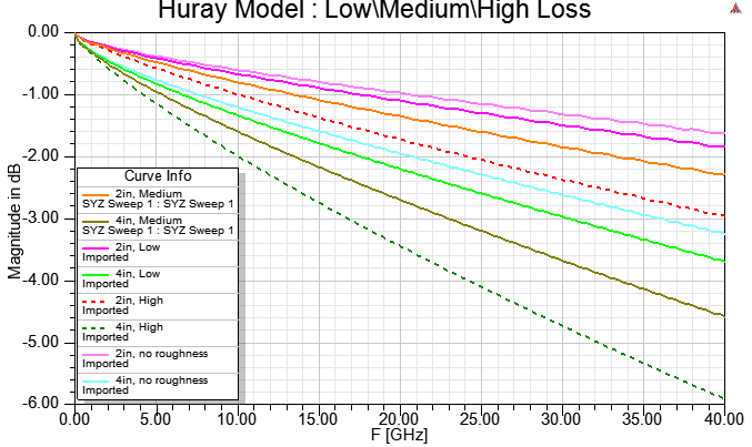
4.2 50 ohm microstrip line, 2 and 4 inch length, trace width 9.9 mils, Dk=3.7, Df=0.004
Bottom side of top layer, Huray roughness model with low\medium\high loss in SIwave
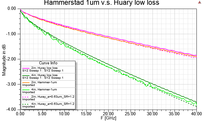
Bottom side of top layer, Hammerstad roughness model (RMS=1um, means low roughness surface).
Bottom side of top layer, Huray roughness model (Nodule Radius=0.63um, Huray Surface Ratio (SR)=1.2)
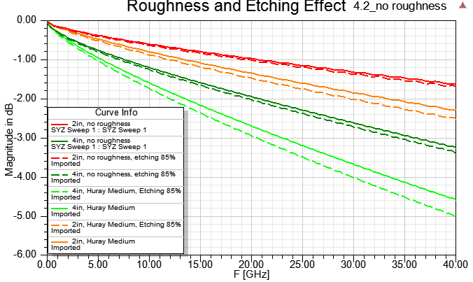
4.3 Etching effect (run with SIwave2016)
-
Roughness model in HFSS
5.1 In HFSS,there are two ways to implement surface roughness
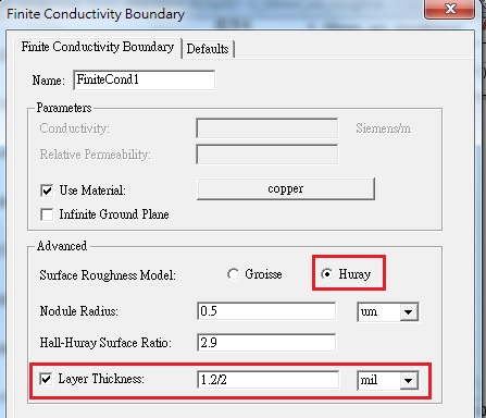
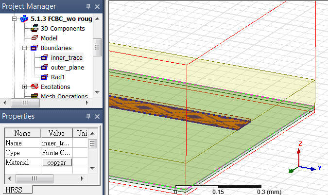
One is [Finite Conductivity] boundary condition (FCBC), this way is popular.
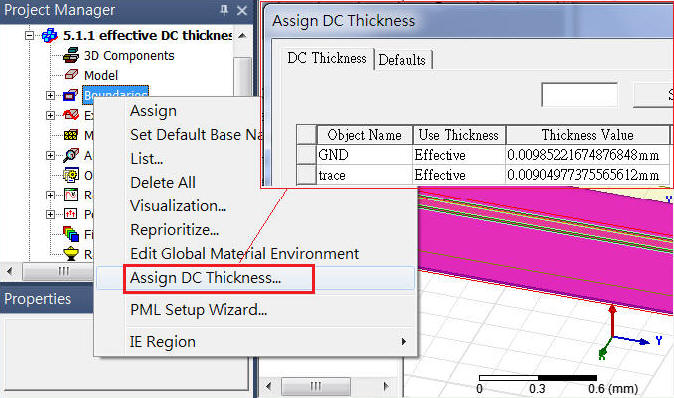
For a good conductor, HFSS doesn't solve inside by default, and automatically solve with [Finite conductivity] on surfaces of the conductor. This happens when skin-effect is active, that is, the conductor thickness is much larger than the skin depth. At the same time, the DC value is solved by [Effective DC Thickness] SBC.
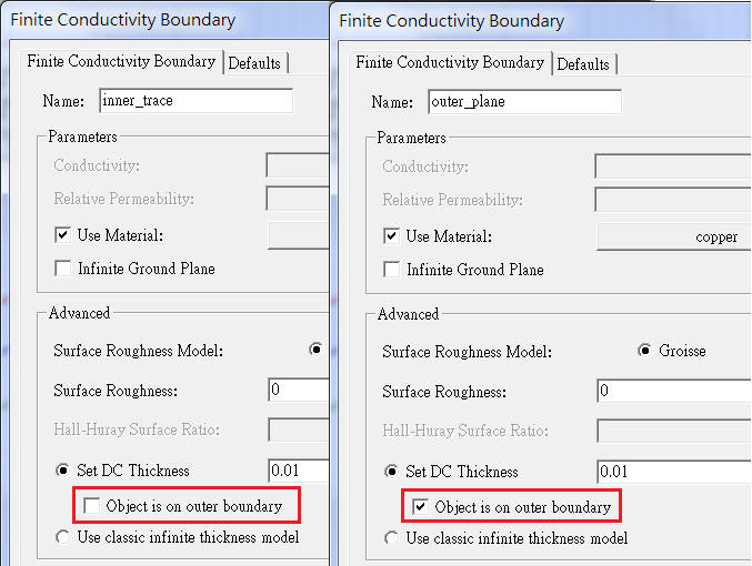
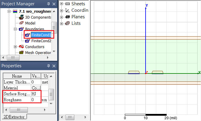
[Effective DC thickness] BC is an inner boundary which is designed for internal surface (as traces), and [Finite conductivity] BC in older version (before 2014) only has outer boundary for outer surface (as ground plane, background plane).
To implement surface roughness BC to traces, in the past, finite conductivity (outer boundary) is the only way. For this case, to be careful ,because for the version before HFSS2014(included), it is just like to implement outer boundary on an internal surface, it will be necessary to divide the conductivity(effective thickness) by two. However, for the version later HFSS2015(included), just leaving [Object is on outer boundary] un-check will be right. refer to 5.1.2, 5.1.4
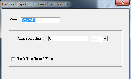
Another way to implement surface roughness in HFSS is [Layered Impedance] boundary condition, LIBC
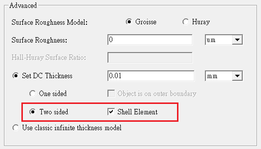
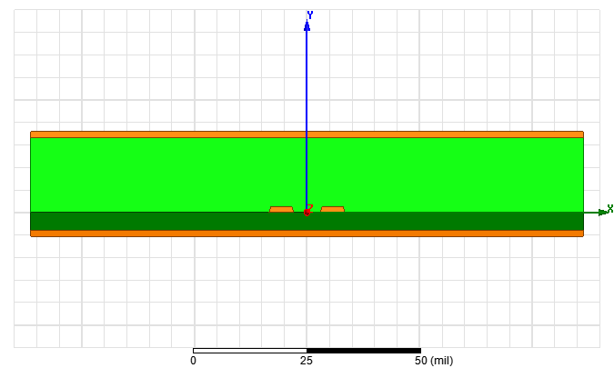
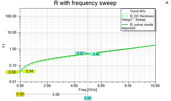
5.1.1 Use solid copper for trace and GND plane, and assign effective DC thickness (this is the suggested method by default).
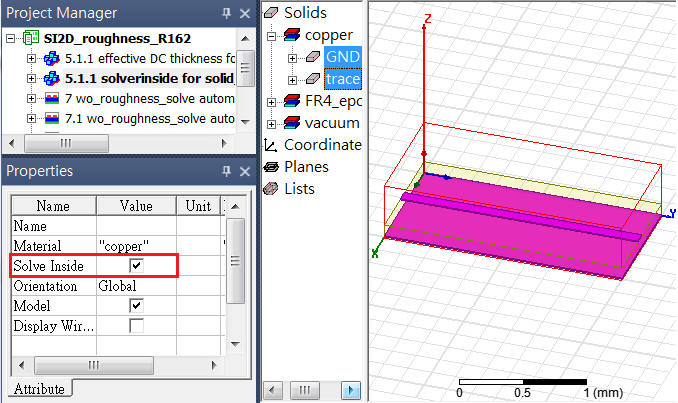
Use solid copper for trace and GND plane, with solve inside (it takes more time, but is used to verify different BC results at low-frequency).
Make sure to have mesh enough when use solver-inside.
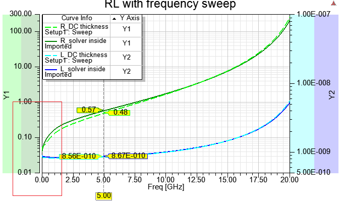
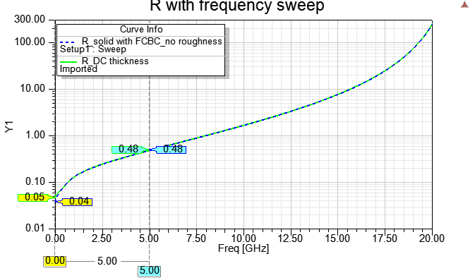
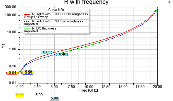
As the previous artical,solving a very thin layer with HFSS, effective DC thickness by default can get the result almost as solver inside at DC.
Based on the picture above, the RDC solved by solver-inside (0.04) is more accurate, however the R5G solved by DC thickness 0.48 is more accurate.
5.1.2 Use sheet copper for trace and GND plane, with FCBC but no roughness (both of trace and plane use inner surface)
HFSS2015 added one more option [Object is on outer boundary] for FCBC. It assigns FCBC to work as inner boundary or outer boundary.
Based on the testing result, the inner/outer boundary option only affects R at low-frequency (~200MHz), and its R is larger than the one solved by solver-inside.
It is because in the version before HFSS2015(included), FCBC only supported one sided BC (i.e. inner\outer BC) which is for the surface of 3D solid object, not for 2D sheet. Please refer to the next section 5.1.3~5.1.4, to implement inner or outer boundary on the surface of 3D object.
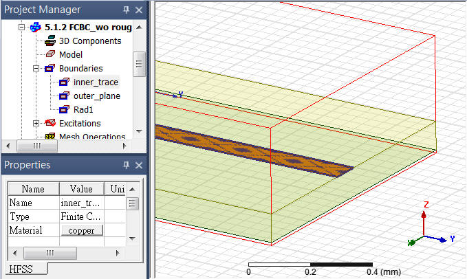
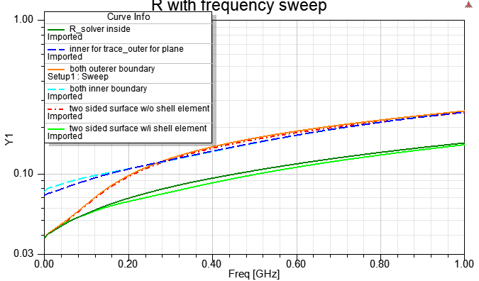
5.1.3 Use solid copper for trace and GND plane, with FCBC but no roughness (inner surface for trace, outer surface for plane)
Now, we meake sure that adding zero roughness by FCBC on a conductor surface,can get the same result as the one by effective DC thickness in 5.1.1, so go on the next step 5.1.4。
5.1.4 Use solid copper for trace and GND plane, with FCBC and Huray roughness
5.2 HFSS simulate TLine with roughness effect,refer to here
5.2.1 For a long transmission line simulation with HFSS, to avoide inaccurate result due to mesh not good enough, please follow the method as below
-- HFSS wave port + de-embedded
5.2.2 There are two papers [4][6] in DesignCon 2014, they all study roughness with HFSS.
Q3D does not support roughness setting, but SI2/D2D solver can.
It seems reasonable for me, since Q3D is Quasi-static solver, for SI application, it is not good at high-frequency (skin-effect region), so roughness setting is unuseful for Q3D.
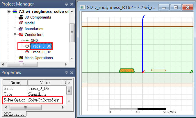
7.1 Assign [Finite Conductivity] boundary on a edge of 2D pattern to implement roughness model for SI2D.
(as HFSS, to implement roughness via [Finite Conductivity] boundary)
7.2 Set [SolveOnBoundary] instead of [Automatic] for the net with roughness setting
-
Q&A
8.1 Does roughness affect L?
Ans:Yes. It affects Z, that is including R and L.
8.2 Does roughness affect DC R?
Ans:After some testing, the answer is NO for SIwave2104, but YES for SIwave2015. (ANSYS enhances solver every year)
In general, the real physical condition is that the profile of roughness is much less than conductor thickness, so the loss contributed by roughness only important when skin-effect is serious.
Even for testing purpose, to continue increasing RMS roughness (or Nodule radius) larger than conductor thickness, the conductor still would not be open, and you can get simulation result, but that is not reliable. Suggest using roughness model for the condition that RMS roughness << conductor thickness. In case, a condition that roughness is close to conductor thickness, to build a real 3D model for simulation is the right way to go. [13][14][15]
8.3 Which roughness model is better?
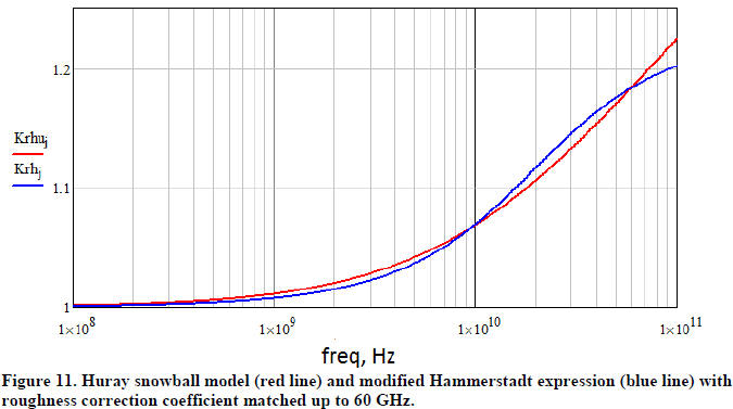
Ans:The effect of Hammerstad and Huray model are similar for low roughness case. [3]p.10,15
(Classic) Hammerstad is only suitable for roughness HRMS<2um, nevertheless, usage of Huray model is unlimited. [2]p.46。In a word, Groisse or Hammerstad model is only for smooth surface usage. For general process and SI(wideband) application, Huray model is proposed. By the way, the slope of Hammerstad model K curve will get saturated at high frequency (30G~).
Below picture shows the two models can get very close effect for low roughness userage. [3]p.10
8.4 How to simulate the resonance absorption valley at 35GHz in step 3.3?
Ans:It is caused by glass weaver effect. [9][10]
8.5 Does SIwave consider surface roughness with "top/bottom" or "top/bottom and side" surface?
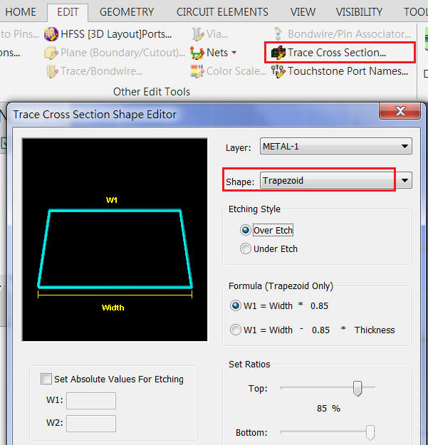
Ans:For conductor with "rectangular" cross section, roughness is applied on top or\and bottom surface. But, for "trapezoid" cross section, top\bottom and slanted sidewalls will be considered.
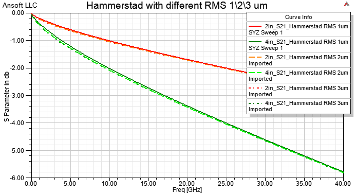
8.6 The Hammerstad used in ANSYS EBU is classic or modified Hammerstad model?
Ans:I beleve it is classic Hammerstad model (ie. the same as Modified Hammerstad model with SF=2)
Hammerstad RMS 1um and 2um are just a bit different, and they are the same between RMS 2um and 3um.
In a word, Groisse and Hammerstad model are ONLY good for smooth surfaces, however, Huray model is good for all surfaces, special for the rougher surface.
8.7 Is it possible to translate the parameter between different roughness model (Hammerstad and Huray)?
Ans:All the roughness models would like to behabve the phenomenon that loss increasing with frequency due to roughness, nevertheless they are the models described by different parameters with different physical meaning. There is no meaningful mathematical transformation relationship based on physics. The best way is to directly compare the S21 or K coefficient results through tuning and fitting.
The ideal simulation method is: to select an appropriate frequency-dependent dielectric model (Djordjevic-Sarkar model, aka Wideband Debye), determine the stackup of the process (Dk, Df, and the cross-section of the transmission line), and obtain the surface roughness measurement value ( for example, Rz) which is roughly divided into low/medium/high roughness, understand the roughness difference between the top surface and the bottom surface, and apply them to the model, compare the results of the S21of testing with the simulation results, and then fine-tune the model Huray model (Nodule radius, Huray Surface Ratio) parameters.
Back to the question of how to use Rz or Ra to the Huray model. Because, in the end, we still need to tune and fit the simulation with measurement, don't be too obsessed with this question. Taking SIwave as an example, it is recommended to start with Nodule radius= 0.5um, with the default three-level low/medium/high roughness setting of Huray Surface Ratio= 1/3/6, and then further fine-tune SR with the S-parameter measurement results parameter.
Why does the SIwave use the three-level roughness setting by a fixed Nodule radius of 0.5 um, and adjust the SR=1/3/6? It can be understood in a physical sense: because a nodule radius represents the smallest unit (snowball) of the snowball model, which is usually not significantly different with different roughness [1]p.12. Using the fixed nodule radius and adjusting the SR, not only can make you call out any roughness but the loss effect is also in line with the physical meaning. In other words: different roughness, generally is implemented by using snowballs of similar size to pile up snowdrifts of different heights, resulting in different losses.
RMS surface roughness
Low (0.5~2um)
Medium (4~6um)
High (8~10um)
Hammerstad Model
RSM=1um
N.A.
N.A.
Huray Model
Nodule radius=0.5um
Huray Surface Ratio=1Nodule radius=0.5um
Huray Surface Ratio=3Nodule radius=0.5um
Huray Surface Ratio=6[11].p.21
Refer to [3]p.10, Hammerstad (RMS=1um,SF=2) is similar to Huray model (a=0.85um, 4*pi*a2*N/Aflat=4*pi*a2*11/65=1.536)
Refer to 4.2 in this article, Hammerstad (RMS=1um, SF=2) is similar to Huray model (a=0.63um, 4*pi*a2*N/Aflat=1.2)
8.8 Is it possible let the result with solver-inside more consistent to effective DC thickness in step 5.1.1?
Ans:
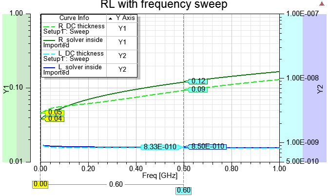
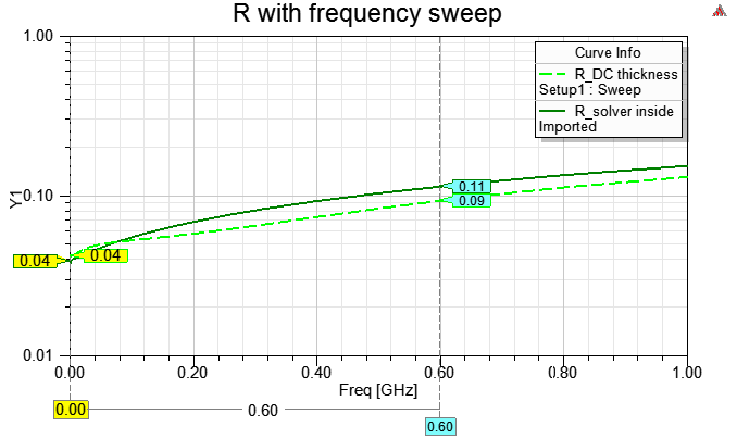
8.8.1 In step 5.1.1, the RDC solved by solver-inside and effective DC thickness are 0.04 and 0.05 ohms respectively. The RDC is 0.04 as a more accurate value. The reason is that under the default setting of effective DC thickness, the conductor thickness of the trace in this example is 0.009mm instead of 0.01mm, which is the main reason for its slightly larger RDC. The conductor thickness can be adjusted back to 0.01mm by manual setting. In addition, make the sampling density of the interpolating sweep better by setting the error tolerance from 0.1% to 0.01%.
Effective DC thickness=2*conductor volume/surface area ... This is the principle for the software to automatically estimate the conductor thickness, which is suitable for thin conductors. But if the conductor thickness is not thin enough relative to the length and width, please input the correct conductor thickness to get a more accurate RDC value.
8.8.2 In step 5.1.1, the R5G value solved by solver-inside is about 0.1 ohm larger than the one by effective DC thickness. It is mainly caused by the mesh performance of the solver inside. Manually add a mesh operation (max.length=0.01mm) setting on the trace object and improve the interpolating sweep by setting error tolerance from 0.1% to 0.01%.
As long as the mesh performance is good enough, the result of solver-inside is reliable, because it solves without the assumption of boundary conditions. However, it takes a much longer time. Generally, solver-inside is only used when shielding effect is required, accurate inductance at low frequencies is required, or review the energy propagated in the conductor. In short, avoid using solver-inside, unless you have a good reason.
After adjusting the above two settings, the following results can be obtained: Compared with 5.1.1, the results are closer.
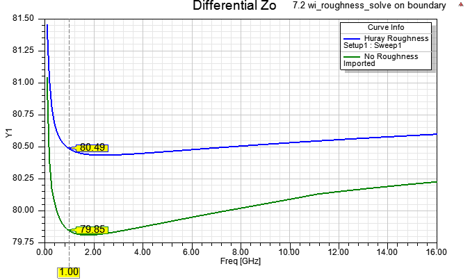
8.9 Why does characteristic impedance Zo increase to infinity while frequency decreases to zero (as 7.2)?
Ans:characteristic impedance
,(G is caused from dielectric loss, usually very small)
For high-frequency,
(the formula is also for the Zo of lossless TLine)
For low frequency,
,when the frequency is close to 0 (w®0),Zo goes to infinity.
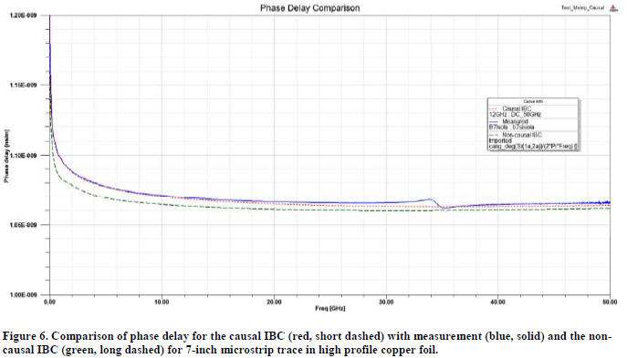
8.10 Does HFSS(finity conductivity) consider the effect of surface roughness with loss and phase constant both?
Ans:Yes, HFSS can do it.
Several years ago, some papers highlighted most of the roughness model did not consider the effect of phase constant (propagation\phase delay). [19]
ANSYS developed a causal Huray model, which did consider both of loss and phase constant well, as below [20].
[1] P.G. Huray, "Impact of Copper Surface Texture on Loss: A Model that Works", DesignCon 2010. (推薦)
[2] Nonideal Conductor Models, p.37~台大吳瑞北教授課程
[3] E. Bogatin, P. Huray, "Which one is better? Comparing Options to Describe Frequency Dependent Losses", DesignCon2013. (推薦)
[4] T. Okubo, T. sudo, "Reducing signal transmission loss by low surface roughness", DesignCon 2014.
[5] 表面粗糙度的定義, Ra, Rz,Rq definition
[6] G. Gold, K. Helmreich, "Effective Conductivity Concept for Modeling Conductor Surface Roughness", DesignCon 2014.
[7] "Elimination of Conductor Foil Roughness Effects in Characterization of Dielectric Properties of PCB", DesignCon 2014.
[8] M. Griesi, P.G. Huray, "Electrodeposited Copper Foil Surface Characterization for Accurate Conductor Loss Modeling", DesignCon 2015. (推薦)
[9] P. Pathmanathan (Intel), P. G. Huray, "Analytic Solutions for Periodically Loaded Transmission Line Modeling", DesignCon 2013.
[10] PCB glass-fiber laminate weave effect
[11] B. Simonovich, "Practical Method for Modeling Conductor Surface Roughness Using Close Packing of Equal Spheres", DesignCon 2015. 另一種較單純的雪球模型
[12] M. Koledintseva, "Effective Roughness Dielectric to Represent Copper Foil Roughness in Printed Circuit Boards", DesignCon 2015.
[13] Milan V. Lukic, "Modeling of 3D Surface Roughness Effects With Application to -Coaxial Lines", IEEE Trans. on Microw. Theory Tech., vol. 55, no. 3, MARCH 2007.
[14] Arghya Sain,"Broadband Characterization of Coplanar Waveguide Interconnects With Rough Conductor Surfaces", IEEE Trans. on Components, Packaging and Manufacturing Technology, vol. 3, no. 6, June 2013. (推薦)
[15] Shaohui Yong, "Advanced Modeling for Novel High-performing Low-cost Copper Foils", DesignCon2021.
[17] Taiwan Union Technology Corporation - IBM, TU-872 low profile
[18] ThunderClad 2/TU-883 - Streamline Circuits, TU-872 low profile
[19] Allen F, "Effect of conductor profile on the insertion loss, phase constant, and dispersion in thin high frequency transmission lines", DesignCon 2010.
[20] J. Eric Bracken, "A Causal Huray Model for Surface Roughness", DesignCon 2012.
專有名詞對照Reverse Treated Copper Foil (RTF), Very Low Profile Copper Foil (VLP), Heavy Copper Foil (HCF)
[21] Yuriy Shlepnev , "Dielectric and Conductor Roughness Models Identification for Successful PCB and Packaging Interconnect Design up to 50 GHz", 2015